M672 데이터 시트보기 (PDF) - Integrated Circuit Systems
부품명
상세내역
일치하는 목록
M672 Datasheet PDF : 4 Pages
| |||
Integrated
Circuit
Systems, Inc.
M672
VCSO WITH SELECTABLE OUTPUT FREQUENCY DIVIDER
Preliminary Information
PIN DESCRIPTIONS
Number Name
1
VIN
2
P_SEL
3
GND
4
FOUT
5
nFOUT
6
VCC
I/O
Input
Input
Ground
Output
Power
Configuration
Internal pull-up resistor1
No internal terminator
Description
Frequency control input.
P Divider selection:
Logic
Logic
0
1
selects
selects
P=1,
P=d,
so
so
that
that
Fout
Fout
=
=
1F/vdcsFov.cso.2
Power supply ground connection.
Clock output pair. Differential LVPECL.
Power supply connection, connect to +3.3V.
Table 2: Pin Descriptions
Note 1: See “P Select Pull-up” in Table 5, DC Characteristics on pg. 3.
Note 2: The P divider value d (4, 8, or 2) is specified as part of the order number. Format is M672-d-xx. See Ordering Information on pg. 4.
ABSOLUTE MAXIMUM RATINGS1
Symbol Parameter
Rating
Unit
VI
Inputs
-0.5 to VCC +0.5
V
VO Outputs
-0.5 to VCC +0.5
V
VCC Power Supply Voltage
TS Storage Temperature
4.6
V
-55 to +125
oC
Table 3: Absolute Maximum Ratings
Note 1: Stresses beyond those listed under Absolute Maximum Ratings may cause permanent damage to the
device. These ratings are stress specifications only. Functional operation of product at these conditions
or any conditions beyond those listed in Recommended Conditions of Operation, DC Characteristics, or
AC Characteristics is not implied. Exposure to absolute maximum rating conditions for extended periods
may affect product reliability.
RECOMMENDED CONDITIONS OF OPERATION
Symbol Parameter
VCC Positive Supply Voltage
TA Ambient Operating Temperature
Min Typ Max Unit
2.97
3.3
3.63
V
-40
25
+85
oC
Table 4: Recommended Conditions of Operation
PARAMETER MEASUREMENT INFORMATION
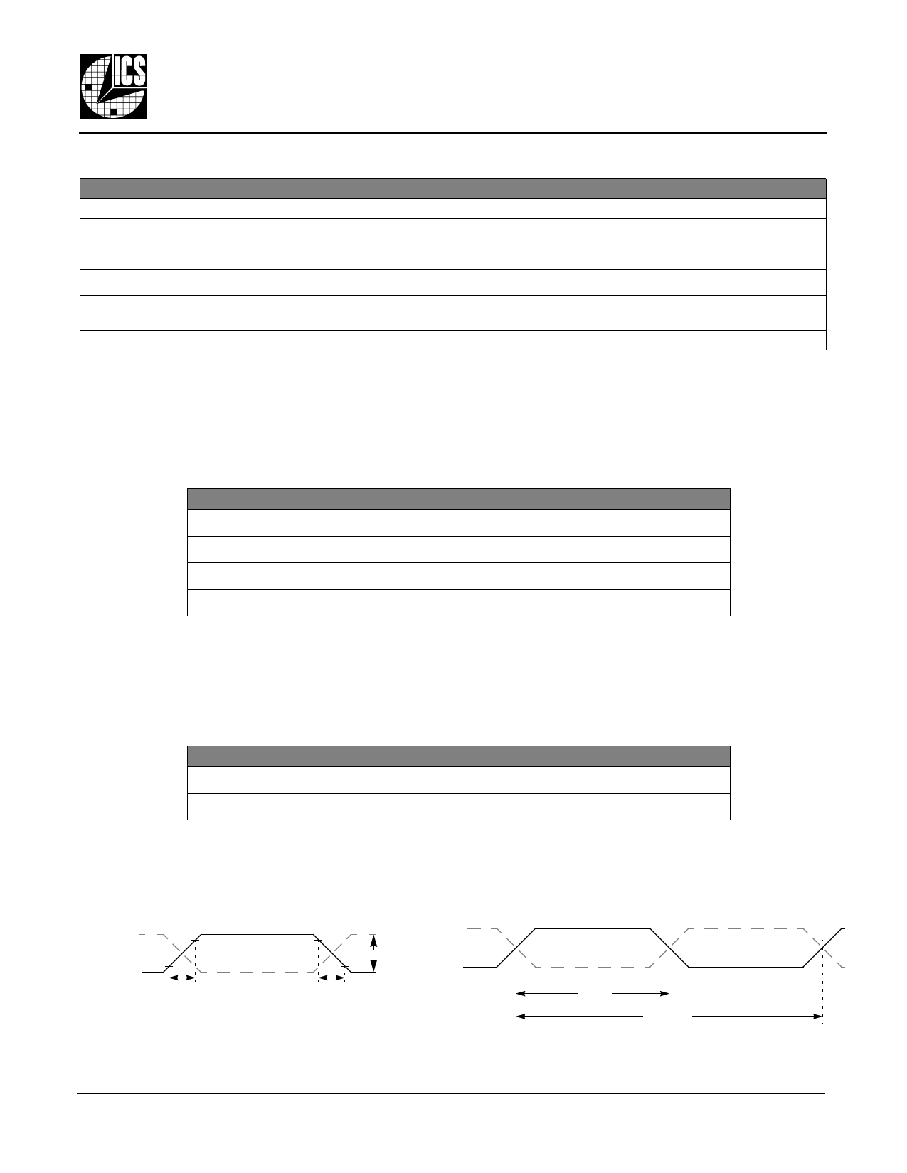
Output Rise and Fall Time
80%
80%
Clock 20%
Outputs
tR
VP-P
20%
tF
Figure 3: Output Rise and Fall Time
Output Duty Cycle
nFOUT
FOUT
tPW
(Output Pulse Width)
odc =
tPW
tPERIOD
tPERIOD
Figure 4: Output Duty Cycle
M672 Datasheet Rev 0.2
2 of 4
Revised 07Apr2004
Integrated Circuit Systems, Inc. ● Communications Modules ● www.icst.com ● tel (508) 852-5400
Share Link: 