M38C88EA-XXXFP 데이터 시트보기 (PDF) - MITSUBISHI ELECTRIC
부품명
상세내역
일치하는 목록
M38C88EA-XXXFP Datasheet PDF : 51 Pages
| |||
PRELIMINARY NSocothimcaene:gpTeah.riasmisetnrioct laimfiintsalasrepescuibfijceacttioton.
MITSUBISHI MICROCOMPUTERS
38C8 Group
SINGLE-CHIP 8-BIT CMOS MICROCOMPUTER
A-D CONVERTER
[A-D Conversion Registers (ADL, ADH)] 003216,
003316
The A-D conversion registers are read-only registers that contain the
result of an A-D conversion. During A-D conversion, do not read these
registers.
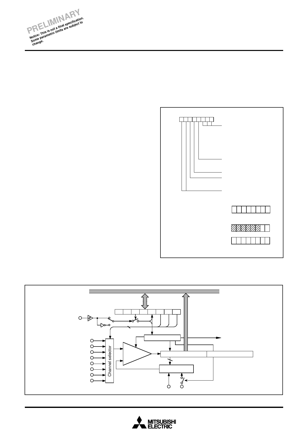
[A-D Control Register (ADCON)] 003116
The A-D control register controls the A-D conversion process. Bits 0
to 2 are analog input pin selection bits. Bit 3 is an A-D conversion
completion bit and “0” during A-D conversion, then changes to “1”
when the A-D conversion is completed. Writing “0” to this bit starts
the A-D conversion. When bit 5, which is the AD external trigger valid
bit, is set to “1”, A-D conversion is started even by a rising edge or
falling edge of an ADT input.
Comparator and Control Circuit
The comparator and control circuit compares an analog input volt-
age with the comparison voltage and stores the result in the A-D
conversion register. When an A-D conversion is completed, the con-
trol circuit sets the AD conversion completion bit and the AD interrupt
request bit to “1”.
Because the comparator consists of a capacitor coupling, a deficient
conversion speed may cause lack of electric charge and make the
conversion accuracy worse. When A-D conversion is performed in
the middle-speed mode or the high-speed mode, set f(XIN) to at least
500 kHz.
In the low-speed mode, A-D conversion is performed by using the
built-in self-oscillation circuit. Therefore, there is no limitation in
the lower bound frequency of f(XIN).
Trigger Start
When using the A-D external trigger, set the port shared with the
ADT pin to input. The polarity of INT1 interrupt edge also applies to
the A-D external trigger. When the INT1 interrupt edge polarity is
switched after an external trigger is validated, an A-D conversion
may be started.
Resistor ladder
The resistor ladder outputs the comparison voltage by dividing the
voltage between VDD and VSS by resistance.
Channel Selector
The channel selector selects one of the ports P33/AIN3–P30/AIN0 and
ports P10/AIN4–P13/AIN7, and inputs it to the comparator.
b7
b0
A-D control register
(ADCON : address 003116)
Analog input pin selection bits
0 0 0 : P30/AIN0
0 0 1 : P31/AIN1
0 1 0 : P32/AIN2
0 1 1 : P33/AIN3
1 0 0 : P10/AIN4
1 0 1 : P11/AIN5
1 1 0 : P12/AIN6
1 1 1 : P13/AIN7
AD conversion completion bit
0 : Conversion in progress
1 : Conversion completed
Not used (return “0” when read)
AD external trigger valid bit
0 : A-D external trigger invalid
1 : A-D external trigger valid
Not used (return “0” when read)
•8-bit read (Read only address 003216.)
A-D conversion register (low-order)
(ADL: Address 003216)
b7
b0
b9 b8 b7 b6 b5 b4 b3 b2
•10-bit read (Read address 003316 first.)
b7
A-D conversion register (high-order)
(ADH: Address 003316)
b0
b9 b8
A-D conversion register (low-order)
(ADL: Address 003216)
b7
b0
b7 b6 b5 b4 b3 b2 b1 b0
Note: High-order 6 bits of address 003316 becomes “0” at reading.
Fig. 25 Structure of A-D control register
Data bus
b7
b0
A-D control register
P41/INT1/ADT
P30/AIN0
P31/AIN1
P32/AIN2
P33/AIN3
P10/AIN4
P11/AIN5
P12/AIN6
P13/AIN7
Fig. 26 A-D converter block diagram
3
A-D control circuit
A-D interrupt request
Comparater
(H)
(L)
A-D conversion register A-D conversion register
10
Resistor ladder
VSS VCC
28
Share Link: 