M24C32-R_05 데이터 시트보기 (PDF) - STMicroelectronics
부품명
상세내역
일치하는 목록
M24C32-R_05 Datasheet PDF : 26 Pages
| |||
M24C64, M24C32
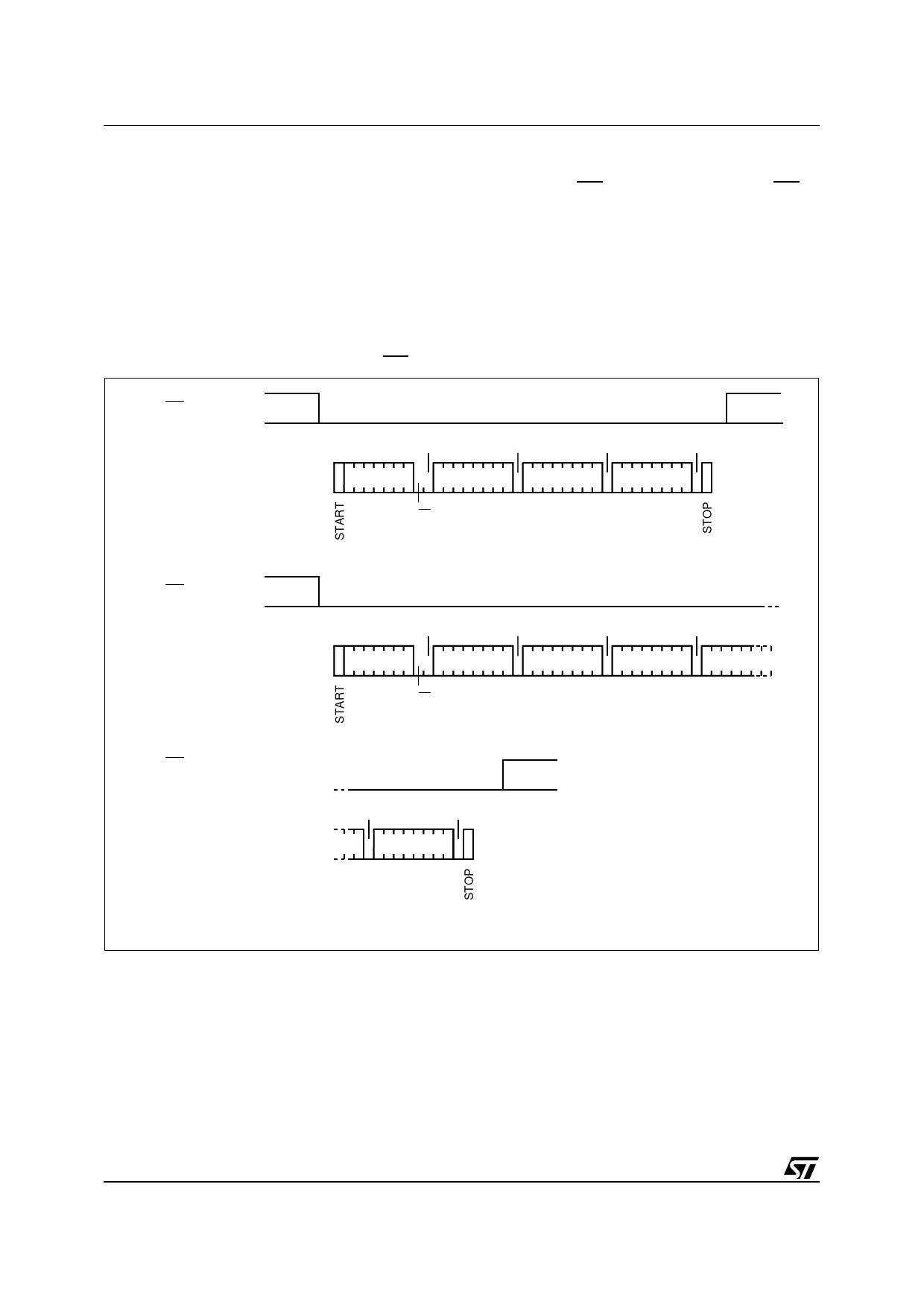
Page Write
The Page Write mode allows up to 32 bytes to be
written in a single Write cycle, provided that they
are all located in the same ’row’ in the memory:
that is, the most significant memory address bits
(b12-b5 for M24C64, and b11-b5 for M24C32) are
the same. If more bytes are sent than will fit up to
the end of the row, a condition known as ‘roll-over’
occurs. This should be avoided, as data starts to
become overwritten in an implementation depen-
dent way.
The bus master sends from 1 to 32 bytes of data,
each of which is acknowledged by the device if
Write Control (WC) is Low. If Write Control (WC) is
High, the contents of the addressed memory loca-
tion are not modified, and each data byte is fol-
lowed by a NoAck. After each byte is transferred,
the internal byte address counter (the 5 least sig-
nificant address bits only) is incremented. The
transfer is terminated by the bus master generat-
ing a Stop condition.
Figure 8. Write Mode Sequences with WC=0 (data write enabled)
WC
BYTE WRITE
ACK
ACK
ACK
ACK
DEV SEL
BYTE ADDR BYTE ADDR
DATA IN
R/W
WC
PAGE WRITE
WC (cont'd)
PAGE WRITE
(cont'd)
ACK
ACK
ACK
ACK
DEV SEL
BYTE ADDR BYTE ADDR DATA IN 1
DATA IN 2
R/W
ACK
ACK
DATA IN N
AI01106C
10/26
Share Link: 