LX8820-33CLM 데이터 시트보기 (PDF) - Microsemi Corporation
부품명
상세내역
일치하는 목록
LX8820-33CLM Datasheet PDF : 6 Pages
| |||
LX8820
®
3.3V/1.0A Ultra Low Dropout Regulator
TM
PRODUCTION DATA SHEET
ABSOLUTE MAXIMUM RATINGS
Input Voltage (VIN) ....................................................................................................... 10V
Load Current (Internally Limited)................................................................................... 2A
Power Dissipation ................................................................................... Internally Limited
Short-Circuit Protection ........................................................................................Indefinite
Operating Junction Temperature................................................................................ 150°C
Storage Temperature Range........................................................................ -65°C to 150°C
RoHS / Pb-free Peak Package Solder Reflow Temperature
(40 second maximum exposure) ....................................................................260°C (+0,-5)
Note: Exceeding these ratings could cause damage to the device. All voltages are with respect to
Ground. Currents are positive into, negative out of specified terminal.
THERMAL DATA
LM Plastic MLP 6-Pin
THERMAL RESISTANCE-JUNCTION TO TAB, θJT
THERMAL RESISTANCE-JUNCTION TO AMBIENT, θJA
(Typical, depending on mounting/pcb layout)
8°C/W
29-35°C/W
Junction Temperature Calculation: TJ = TA + (PD x θJA).
The θJA numbers are guidelines for the thermal performance of the device/pc-board
system. All of the above assume no ambient airflow. θJA can vary significantly depending
on mounting technique. (See Application Notes Section: Thermal considerations)
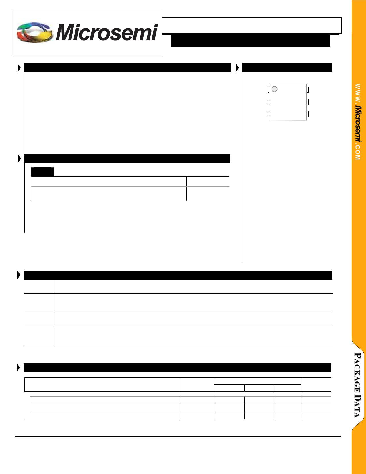
PACKAGE PIN OUT
VIN 1
GND 2
N.C. 3
6 VIN
5 VOUT
4 VOUT
LM PACKAGE
(Top View)
Heatsink must be connected to GND
or left floating (see pg 7 for details)
. N/C = Not internally connected, don’t
care for PCB layout consideration.
RoHS / Pb-free 100% Matte Tin Lead Finish
PIN NAME
VIN
GND
VOUT
FUNCTIONAL PIN DESCRIPTION
DESCRIPTION
Positive unregulated supply input for the regulator. Bypass to GND with at least 2.2µF of low ESR and ESL
capacitance.
Common terminal for ground reference. The input and output bypass capacitors should be connected to this
pin.
Regulator output. It is recommended to bypass to GND with at least 2.2µF. Size your output capacitor to meet
the transient loading requirement. If you have a very dynamic load, a lower ESR capacitor will improve the
response to these load steps.
RECOMMENDED MAX OPERATING CONDITIONS
Parameter
Symbol
LX8820-33
Min
Typ
Input Voltage
Load Current (with adequate heat sinking)
Operating Junction Temperature
VIN
4.5
IL
TJ
Max
10
1200
125
Units
V
mA
°C
Copyright © 2004
Rev. 1.1, 2005-02-24
Microsemi
Integrated Products Division
11861 Western Avenue, Garden Grove, CA. 92841, 714-898-8121, Fax: 714-893-2570
Page 2
Share Link: 