OMS405A 데이터 시트보기 (PDF) - Omnirel Corp => IRF
부품명
상세내역
일치하는 목록
OMS405A
Omnirel Corp => IRF

OMS405A Datasheet PDF : 4 Pages
| |||
OMS305, OMS305A, OMS405
2.1
ELECTRICAL CHARACTERISTICS: OMS405 (TC = 25° unless otherwise specified)
Characteristic
Symbol
Min.
OFF CHARACTERISTICS
Drain-Source Breakdown Voltage, ID = 250 µA, VGS = 0
V(BRDSS
50
Zero Gate Voltage Drain Current = VGS, VDS = Max. Rat.
IDSS
-
VDS = Max. Rat. x 0.8, TC = 70°C
-
Gate-Body Leakage, VGS = ±12 V
IGSS
-
ON CHARACTERISTICS
Gate-Threshold Voltage, VDS = VGS, ID = 250 µA
Static Drain-Source On-Resistance, VGS = 10 Vdc, ID = 22.5 A
Static Drain-Source On-Resistance TC = 70°C
On State Drain Current, VDS > ID(on X RDS(on) Max., VGS = 10
VGS(th)
2.0
RDS(on)
-
-
ID(on)
45
DYNAMIC CHARACTERISTICS
Forward Transconductance
VDS > ID(on) X RDS(on) Max., ID = 40 A,
gfs
25
Input Capacitance
VDS = 25 V,
Ciss
-
Output Capacitance
VGS = 0,
Coss
-
Reverse Transfer Capacitance
f = 1.0 mHz
Crss
-
SWITCHING CHARACTERISTICS
Turn-On Delay Time
Rise Time
Turn-Off Delay Time
Fall Time
VDD = 30 V, ID = 45 A,
td(on)
-
ID = 10 A,
tr
-
RGS = 50 , VGS = 10 V
td(off)
-
tf
-
SOURCE DRAIN DIODE CHARACTERISTICS
Source - Drain Current
Source - Drain Current (Pulsed)
Forward On-Voltage
Reverse Recovery Time
Reverse Recovered Charge
ISD
-
ISDM*
-
ISD = 45 A, VGS = 0,
VSD
-
ISD = 45 A,
trr
-
di/dt = 100 A/µSec
Qrr
-
RESISTOR CHARACTERISTICS
Resistor Tolerance
Temperature Coefficient, -40°C to +70°C
RS
9.0
Tcr
-
* Indicates Pulse Test 300 µsec, Duty Cycle 1.5%.
Typ.
Max.
Unit
-
-
V
-
250
µA
-
750
µA
-
±100
nA
-
4.0
V
-
0.016
-
0.028
-
-
A
-
-
mho
-
5200
pF
-
2300
pF
-
600
pF
-
260
ns
-
1200
ns
-
550
ns
-
420
ns
-
45
A
-
150
A
-
1.5
V
120
-
ns
0.45
-
µC
10
11
m
100
-
ppm
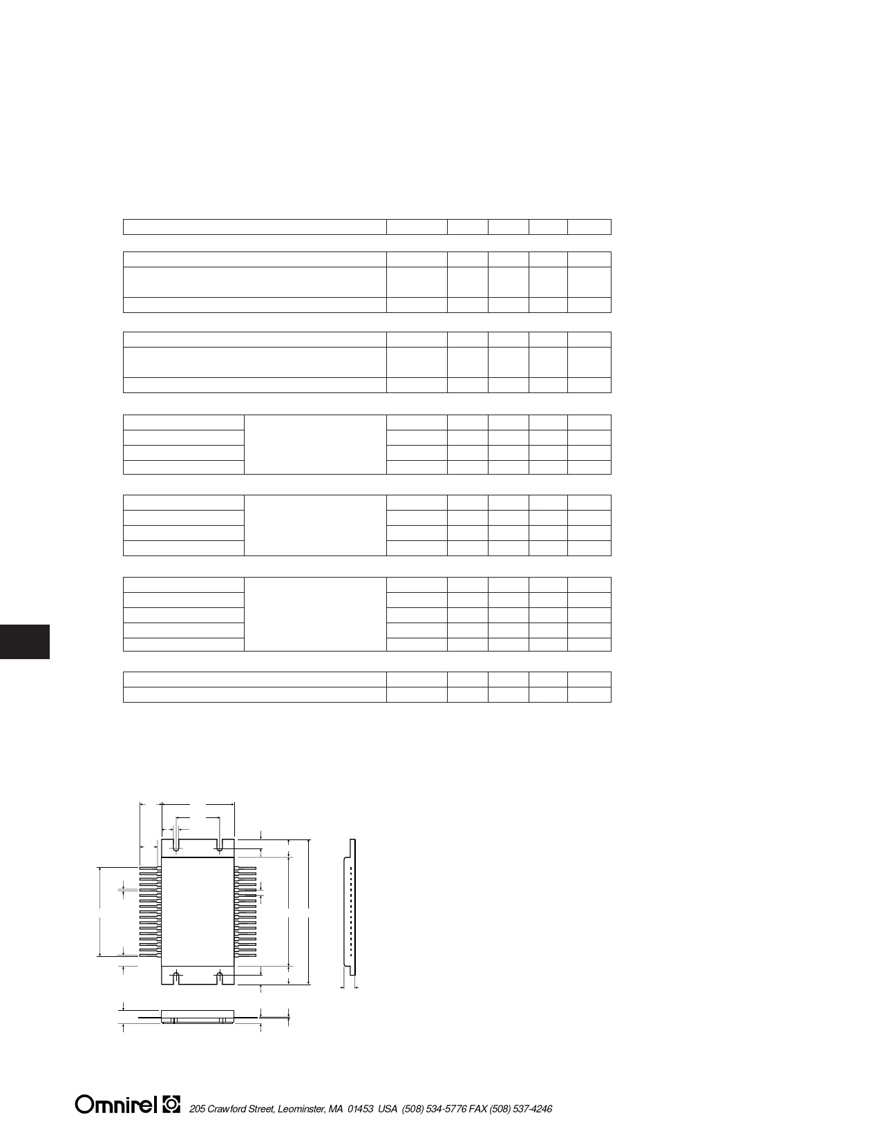
Mechanical Outline
.600
.325
.135
2.000
1.350
.150
(4) PLCS.
.050
1
(34) PLCS.
2.450
.250
.500
.150
3.000 4.000
.300
.360 MAX.
.500
.250
.360
.020
.180
Pin 1: Gate Q1
Pin 2: Source Q1
Pin 3: Gate Q2
Pin 4: Source Q2
Pin 5: Gate Q3
Pin 6: Source Q3
Pin 7: Gate Q4
Pin 8: Source Q4
Pin 9: Gate Q5
Pin 10: Source Q5
Pin 11: Gate Q6
Pin 12: Source Q6
Pin 13: +Sense Res.
Pin 14: -Sense Res.
Pin 15: Power GND
Pin 16: Power GND
Pin 17: Power GND
Pin 34: VDD
Pin 33: VDD
Pin 32: VDD
Pin 31: Output Phase A
Pin 30: Output Phase A
Pin 29: Output Phase A
Pin 28: Output Phase B
Pin 17: Output Phase B
Pin 26: Output Phase B
Pin 25: Output Phase C
Pin 24: Output Phase C
Pin 23: Output Phase C
Pin 22: +PTC
Pin 21: -PTC
Pin 20: Power GND
Pin 19: Power GND
Pin 18: Power GND
Contact factory for lead bending options.
Mounting Recommendations: Maximum Mounting Torque: 3.0 mN. The module must be attached to a flat heat sink (flatness 100um maximum).
205 Crawford Street, Leominster, MA 01453 USA (508) 534-5776 FAX (508) 537-4246
Share Link: