LX1676(2005) 데이터 시트보기 (PDF) - Microsemi Corporation
부품명
상세내역
일치하는 목록
LX1676 Datasheet PDF : 16 Pages
| |||
LX1676
TM
®
Mobile AMD Athlon™ VRM Controller
PRODUCTION DATA SHEET
THEORY OF OPERATION
GENERAL DESCRIPTION
The LX1676 is a voltage-mode pulse-width modulation
controller integrated circuit. The PWM frequency is
programmable from 200kHz to 1MHz. The device has
external compensation, for more flexibility of the loop
response. The LX1676 also makes use of a true differential
input amplifier for remote voltage sensing at the actual
processor core. This is a very important feature now that
the core voltages are in the 1 to 2 volt range. The reference
for the biphase PWM output is a 5 bit VID code DAC. The
VID code DAC can generate a reference voltage of 0.925 to
2.000 volts. The output of the DAC is a bi-directional
current source and is connected to the DACOUT pin.
Connecting a capacitor from this pin to ground will
generate a linear ramp, which will determine the rate of
change of the output voltage. The rate of change can be set
so that the current required to charge the total output
capacitance is below the maximum current limit trip point.
This will allow VID changes on the fly without tripping the
over current sensor.
POWER UP AND INITIALIZATION
At power up, the LX1676 monitors the supply voltage to
VCC and Vin, Before both supplies reach their under-
voltage lock-out (UVLO) thresholds, a power on reset
condition will prevent soft-start from beginning, the
oscillator is disabled and all MOSFETs are kept off.
SOFT-START
Once the supplies are above the UVLO threshold and the
Enable pin is brought high, the soft-start capacitor begins to
be charged up by the reference DAC through the DACOUT
pin. The capacitor voltage at the DACOUT pin rises as a
linear ramp. The DACOUT pin is connected to the error
amplifier’s non-inverting input which controls the output
voltage. The output voltage will follow the DACOUT pin
voltage.
Phase 3 (hysteretic phase) is disabled during soft-start.
OVER-CURRENT PROTECTION
There are two separate current limit circuits in the
LX1676. One looks at the phase 1 lower MOSFET drain
current and the second looks at the phase 3 upper MOSFET
drain current. Both circuits have a 400 nS delay before a
current limit command is issued to the current limit latch,
once set the current limit latch will hold all three phases off
until it is reset.
The Over-Current Protection is disabled during positive
VID changes.
To reset the current limit latch either the enable command
(ENA) must be cycled low then back high or the input
power must cycle off and then back on.
OVER-CURRENT PROTECTION (PHASE 1)
The phase 1 current limit uses the RDS(ON) of the
lower MOSFET, together with a resistor (RSET) to set the
actual current limit point. The current limit comparator
senses the current 400 nS after the lower MOSFET is
switched on. A current source supplies a current (ISET),
of 50µA which flows into RSET and determines the
current limit trip point. The value of RSET is selected to
set the current limit for the application.
Phase 1 RSET is calculated by:
RSET
=
ILimit • RDS(ON)
50 µA
The current limit comparator will trip when the drop
across RSET equals the drop across the lower MOSFET
RDS(ON)., at this time the comparator outputs a signal to
set the I limit latch and removes the enable command. The
Over-Current sensing is done on phase 1 only because
phase 2 current is always being forced to equal the phase
1 current, therefore the current trip point is set at half of the
desired current limit. For an output current limit setting of
30 amps, the current trip point for phase 1 is set at 15
amps.
When the phase 1 over current latch is set all three
phases are disabled, all MOSFETs are turned off.
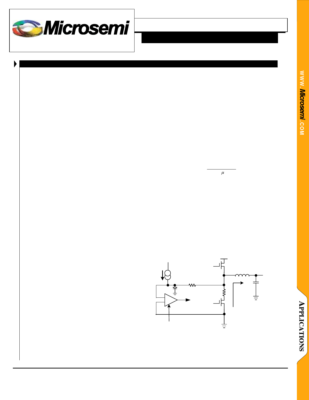
Vin
50 uA
Q1
Vout
+ _ RSET
_
+ Current Limit
Comparator
400nSec Delay
_ Iout
RDS(ON)
+
Q2
Q2
Current
Flow
Figure 3 – Phase 1 Current Limit
The delay before current limit is activated will result in
current pulses exceeding the calculated values during the
delay period if a short circuit is applied during that time.
Copyright © 2000
Revision: 1.0, 4/12/2005
Microsemi
Integrated Products Division
11861 Western Avenue, Garden Grove, CA. 92841, 714-898-8121, Fax: 714-893-2570
Page 9
Share Link: 