LTC3542I 데이터 시트보기 (PDF) - Linear Technology
부품명
상세내역
일치하는 목록
LTC3542I Datasheet PDF : 16 Pages
| |||
LTC3542
PIN FUNCTIONS (DFN/TSOT-23)
VFB (Pin 1/Pin 3): Output Feedback Pin. Receives the
feedback voltage from an external resistive divider across
the output. Nominal voltage for this pin is 0.6V.
VIN (Pin 2/Pin 1): Power Supply Pin. Must be closely
decoupled to GND.
GND (Pin 3/Pin 2): Ground Pin.
SW (Pin 4/Pin 6): Switch Node Connection to Inductor.
This pin connects to the drains of the internal main and
synchronous power MOSFET switches.
MODE/SYNC (Pin 5/Pin 5): Mode Selection and Oscillator
Synchronization Pin. This pin controls the operation of the
device. When tied to GND or VIN, Burst Mode operation or
pulse skipping mode is selected, respectively. Do not float
this pin. The oscillation frequency can be synchronized to
an external oscillator applied to this pin and pulse skipping
mode is automatically selected.
RUN (Pin 6/Pin 4): Converter Enable Pin. Forcing this pin
above 1.5V enables this part, while forcing it below 0.3V
causes the device to shut down. In shutdown, all functions
are disabled drawing <1μA supply current. This pin must
be driven; do not float.
GND (Pin 7, DFN Package Only): Exposed Pad. The Ex-
posed Pad is ground. It must be soldered to PCB ground
to provide both electrical contact and optimum thermal
performance.
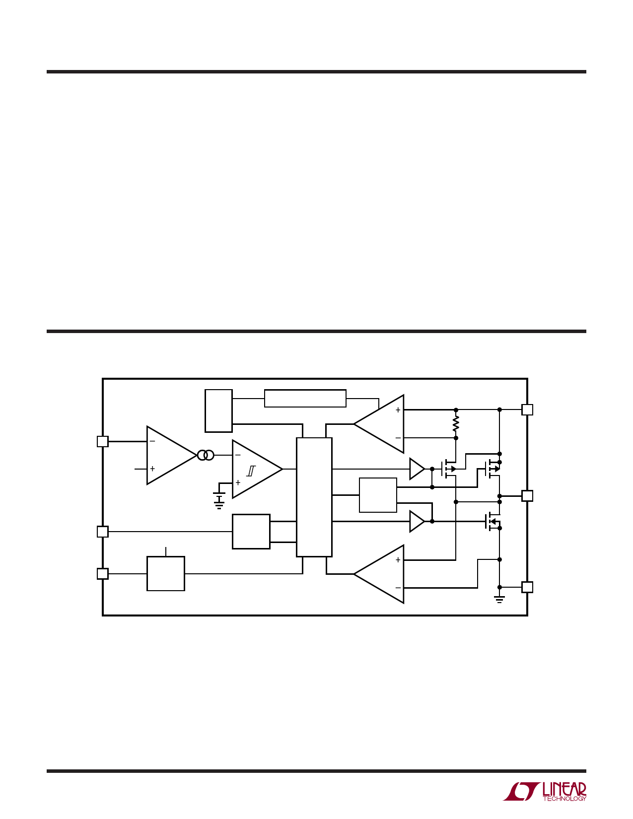
BLOCK DIAGRAM
VFB
0.6V
–
EA
+
MODE/SYNC
VIN
SLOPE COMPENSATION
OSC
–
+
VB
+
BURST
LOGIC
MODE
DETECT
MODE
CLKIN
RUN
SHUTDOWN
0.6V REF
ICOMP
ANTI-
SHOOT
THROUGH
IRCMP
VIN
SW
GND
3542 BD
3542fa
6
Share Link: 