LTC1751-5 데이터 시트보기 (PDF) - Linear Technology
부품명
상세내역
일치하는 목록
LTC1751-5 Datasheet PDF : 12 Pages
| |||
LTC1751/LTC1751-3.3/LTC1751-5
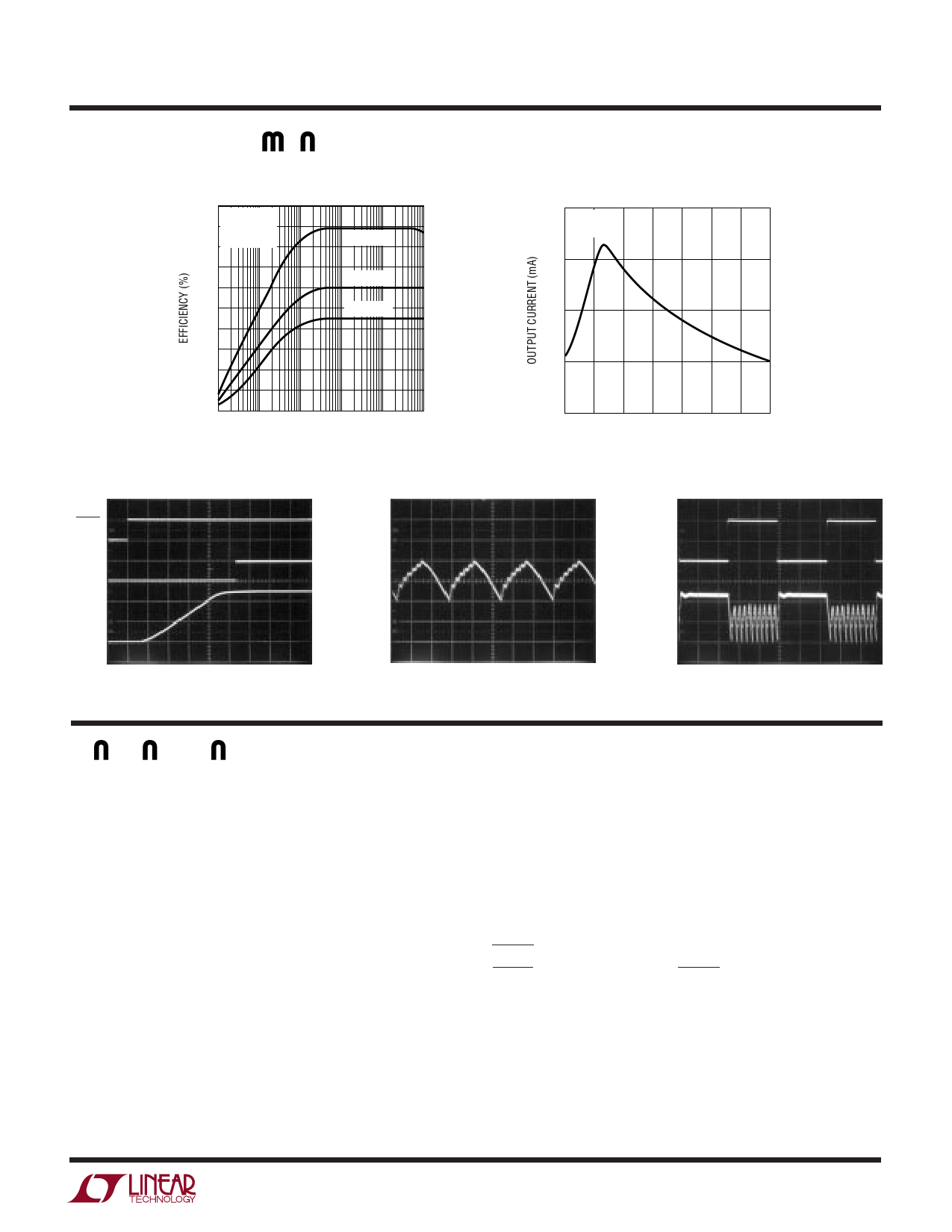
TYPICAL PERFOR A CE CHARACTERISTICS
(LTC1751-5)
Power Efficiency vs Load Current
100
TA = 25°C
90 CFLY = 1µF
80 COUT = 10µF
VIN = 2.7V
70
VIN = 4.1V
60
Short-Circuit Output Current
vs Input Voltage
250
TA = 25°C
CFLY = 1µF
200
50
VIN = 5.5V
150
40
30
100
20
10
0
0.001
0.01 0.1
1
10 100
LOAD CURRENT (mA)
1751 G11
50
2.0 2.5
3.0 3.5 4.0 4.5
INPUT VOLTAGE (V)
5.0 5.5
1751 G12
Start-Up
Output Ripple
Load Transient Response
SHDN
2V/DIV
PGOOD
5V/DIV
VOUT
2V/DIV
VOUT
AC COUPLED
50mV/DIV
IOUT
50mA/DIV
VOUT
AC COUPLED
50mV/DIV
CSS = 10nF
2ms/DIV
1751 G13
VIN = 3V
IOUT = 100mA
COUT = 10µF
5µs/DIV
1751 G14
VIN = 3V
50µs/DIV
1751 G15
PI FU CTIO S
PGOOD (Pin 1) (LTC1751-3.3/LTC1751-5): Output Volt-
age Status Indicator. On start-up, this open-drain pin re-
mains low until the output voltage, VOUT, is within 4.5%
(typ) of its final value. Once VOUT is valid, PGOOD becomes
high-Z. If, due to a fault condition, VOUT falls 7% (typ) below
its correct regulation level, PGOOD pulls low. PGOOD may
be pulled up through an external resistor to any appropri-
ate reference level.
FB (Pin 1) (LTC1751): The voltage on this pin is compared
to the internal reference voltage (1.205V) by the error
comparator to keep the output in regulation. An external
resistor divider is required between VOUT and FB to pro-
gram the output voltage.
VOUT (Pin 2): Regulated Output Voltage. For best perfor-
mance, VOUT should be bypassed with a 6.8µF (min) low
ESR capacitor as close to the pin as possible .
VIN (Pin 3): Input Supply Voltage. VIN should be bypassed
with a 6.8µF (min) low ESR capacitor.
GND (Pin 4): Ground. Should be tied to a ground plane for
best performance.
C – (Pin 5): Flying Capacitor Negative Terminal.
C+ (PIN 6): Flying Capacitor Positive Terminal.
SHDN (Pin 7): Active Low Shutdown Input. A low on
SHDN disables the device. SHDN must not be allowed to
float.
SS (Pin 8): Soft-Start Programming Pin. A capacitor on SS
programs the start-up time of the charge pump so that
large start-up input current is eliminated.
5
Share Link: 