LTC1522CMS8 데이터 시트보기 (PDF) - Linear Technology
부품명
상세내역
일치하는 목록
LTC1522CMS8 Datasheet PDF : 8 Pages
| |||
LTC1522
APPLICATIONS INFORMATION
A ceramic capacitor is recommended for the flying capaci-
tor with a value in the range of 0.1µF to 0.22µF. Note that
a large value flying cap (> 0.22µF) will increase output
ripple unless COUT is also increased. For very low load
applications, CFLY may be reduced to 0.01µF to 0.047µF.
This will reduce output ripple at the expense of efficiency
and maximum output current.
Output Ripple
Normal LTC1522 operation produces voltage ripple on the
VOUT pin. Output voltage ripple is required for the LTC1522
to regulate. Low frequency ripple exists due to the hyster-
esis in the sense comparator and propagation delays in the
charge pump enable/disable circuits. High frequency ripple
is also present mainly due to ESR (Equivalent Series
Resistance) in the output capacitor. Typical output ripple
under maximum load is 50mVP-P with a low ESR 10µF
output capacitor.
The magnitude of the ripple voltage depends on several
factors. High input voltages (VIN > 3.3V) increase the output
ripple since more charge is delivered to COUT per clock
cycle. A large flying capacitor (> 0.22µF) also increases
ripple for the same reason. Large output current load and/
or a small output capacitor (< 10µF) results in higher ripple
due to higher output voltage dV/dt. High ESR capacitors
(ESR > 0.5Ω) on the output pin cause high frequency
voltage spikes on VOUT with every clock cycle.
There are several ways to reduce the output voltage ripple.
A larger COUT capacitor (22µF or greater) will reduce both
the low and high frequency ripple due to the lower COUT
charging and discharging dV/dt and the lower ESR typi-
cally found with higher value (larger case size) capacitors.
A low ESR ceramic output capacitor will minimize the high
frequency ripple, but will not reduce the low frequency
ripple unless a high capacitance value is chosen. A reason-
able compromise is to use a 10µF to 22µF tantalum
capacitor in parallel with a 1µF to 3.3µF ceramic capacitor
on VOUT to reduce both the low and high frequency ripple.
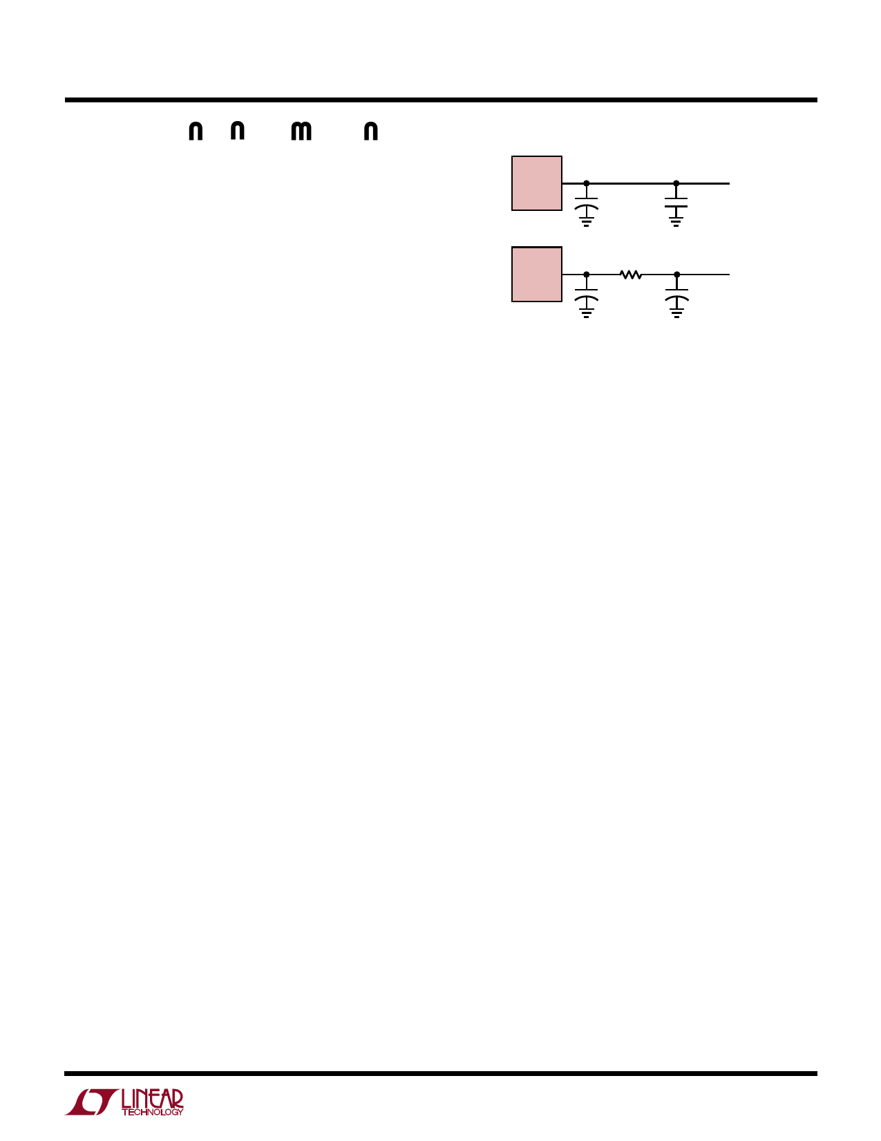
An RC filter may also be used to reduce high frequency
voltage spikes (see Figure 1).
LTC1522
3
VOUT +
15µF
TANTALUM
VOUT
5V
1µF
CERAMIC
LTC1522
3
VOUT +
3.9Ω
10µF
+
TANTALUM
VOUT
5V
10µF
TANTALUM
1522 F01
Figure 1. Output Ripple Reduction Techniques
In low load or high VIN applications, smaller values for
CFLY may be used to reduce output ripple. A smaller flying
capacitor (0.01µF to 0.047µF) delivers less charge per
clock cycle to the output capacitor resulting in lower
output ripple. However, the smaller value flying caps also
reduce the maximum IOUT capability as well as efficiency.
Inrush Currents
During normal operation, VIN will experience current tran-
sients in the 50mA to 100mA range whenever the charge
pump is enabled. During start-up, these inrush currents
may approach 250mA. For this reason, it is important to
minimize the source resistance between the input supply
and the VIN pin. Too much source resistance may result in
regulation problems or even prevent start-up.
Ultralow Quiescent Current (IQ = 2.1µA)
Regulated Supply
The LTC1522 contains an internal resistor divider (refer to
the Block Diagram) that draws only 1µA (typ) from VOUT.
During no-load conditions, the internal load causes a
droop rate of only 100mV per second on VOUT with
COUT = 10µF. Applying a 2Hz to 100Hz, 95% to 98% duty
cycle signal to the SHDN pin ensures that the circuit of
Figure 2 comes out of shutdown frequently enough to
maintain regulation during no-load or low-load condi-
tions. Since the part spends nearly all of its time in
shutdown, the no-load quiescent current (see Figure 3a) is
approximately equal to (VOUT)(1µA)/(VIN)(Efficiency).
5
Share Link: 