LT3464 데이터 시트보기 (PDF) - Linear Technology
부품명
상세내역
일치하는 목록
LT3464 Datasheet PDF : 16 Pages
| |||

LT3464
APPLICATIO S I FOR ATIO
Capacitor Selection
The small size and low ESR of ceramic capacitors makes
them suitable for LT3464 applications. X5R and X7R types
are recommended because they retain their capacitance
over wider voltage and temperature ranges than other
types such as Y5V or Z5U. A 1µF input capacitor and a
0.22µF to 0.47µF output capacitor are sufficient for most
LT3464 applications. Always use a capacitor with a suffi-
cient voltage rating. Table 2 shows a list of several capaci-
tor manufacturers. Consult the manufacturers for more
detailed information and for their entire selection of related
parts.
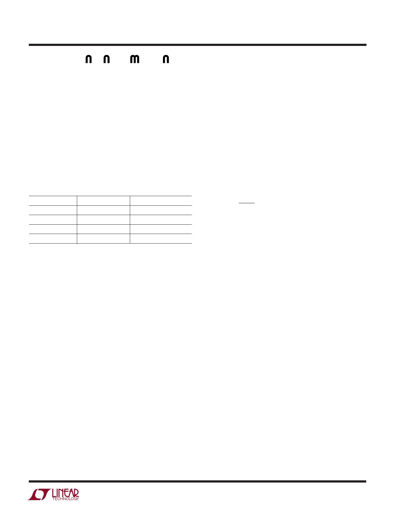
Table 2. Recommended Ceramic Capacitor Manufacturers
MANUFACTURER
PHONE
URL
Taiyo Yuden
408-573-4150
www.t-yuden.com
AVX
843-448-9411
www.avxcorp.com
Murata
814-237-1431
www.murata.com
Kemet
408-986-0424
www.kemet.com
Output Voltage Ripple
Using low ESR capacitors will help minimize the output
ripple voltage, but proper selection of the inductor and the
output capacitor also plays a big role. The LT3464 pro-
vides energy to the load in bursts by ramping up the
inductor current, then delivering that current to the load.
If too large an inductor value or too small a capacitor value
is used, the output ripple voltage will increase because the
capacitor will be slightly overcharged each burst cycle. To
reduce this effect, a larger output capacitor may be used.
The LT3464 also includes an on-chip phase-lead capacitor
between the CAP pin and the FB pin to greatly reduce
ripple; however, certain applications can benefit from
additional capacitance in parallel with the integrated ca-
pacitor, which may be added externally between the CAP
and FB pins. Typical effective values range from 4.7pF to
20pF. Since the FB pin sits at a low voltage, be sure the
chosen capacitor has a sufficient voltage rating.
Setting Output Voltage and the
Auxiliary Reference Input
The LT3464 is equipped with both an internal 1.25V
reference and an auxiliary reference input. This allows the
user to select between using the built-in reference, and
supplying an external reference voltage. The voltage at the
CTRL pin can be adjusted while the chip is operating to
alter the output voltage of the LT3464 for purposes such
as display dimming or contrast adjustment. To use the
internal 1.25V reference, the CTRL pin must be held higher
than 1.5V, which can be done by tying it to VIN. When the
CTRL pin is held between 0V and 1.2V the LT3464 will
regulate the output such that the FB pin voltage is equal to
the CTRL pin voltage.
To set the output voltage, select the values of R1 and R2
according to the following equation (see Figure 4).
R2
=
R1
VOUT
VREF
– 1
Where VREF =1.25V if the internal reference is used, or
VREF = VCTRL if VCTRL is between 0V and 1.2V.
Choosing a Feedback Node
The top of the feedback divider may be connected to the
OUT pin or to the CAP pin (see Figure 4). Regulating the
OUT pin eliminates the output offset resulting from the
voltage drop across the output disconnect. However, in
the case of a short-circuit fault at the OUT pin, the LT3464
will switch continuously because the FB pin is low. While
operating in this open-loop condition, the rising voltage at
the CAP pin is limited only by the current limit of the output
disconnect. Given worst-case parameters this voltage
may reach 25V. When the short-circuit is removed, the
OUT pin will bounce up to the voltage on the CAP pin,
potentially exceeding the set output voltage until the
capacitor voltages fall back into regulation. While this is
harmless to the LT3464, this should be considered in the
context of the external circuitry if short-circuit events are
expected.
Regulating the CAP pin ensures that the voltage on the
OUT pin never exceeds the set output voltage after a short-
circuit event. However, this setup does not compensate
for the voltage drop across the output disconnect, result-
ing in an output voltage that is slightly lower than the
voltage set by the resistor divider. The next section dis-
cusses how to compensate for this drop.
3464f
9