LT1521 데이터 시트보기 (PDF) - Linear Technology
부품명
상세내역
일치하는 목록
LT1521 Datasheet PDF : 16 Pages
| |||
LT1521/LT1521-3
LT1521-3.3/LT1521-5
APPLICATIONS INFORMATION
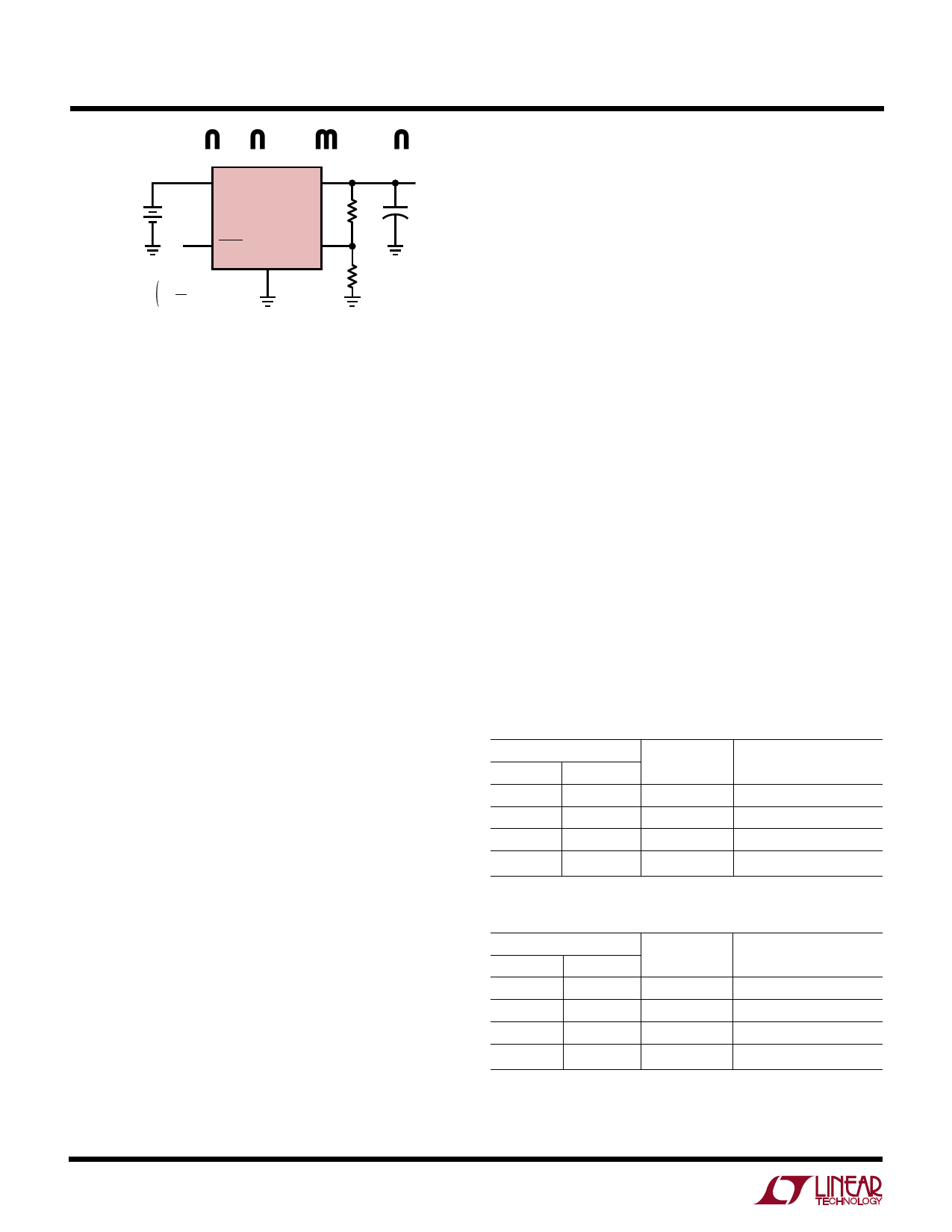
IN
OUT
VIN
LT1521
+
R2
VOUT
SHDN
ADJ
GND
) VOUT = 3.75V
1 + R2
R1
+ (IADJ + R2)
R1
VADJ = 3.75V
IADJ = 50nA AT 25°C
OUTPUT RANGE = 3.75V TO 20V
Figure 2. Adjustable Operation
LT1521 • F01
output is turned off and the divider current will be zero.
Curves of Adjust Pin Voltage vs Temperature and Adjust
Pin Bias Current vs Temperature appear in the Typical
Performance Characteristics. The reference voltage at the
adjust pin has a positive temperature coefficient of ap-
proximately 15ppm/°C. The adjust pin bias current has a
negative temperature coefficient. These effects will tend to
cancel each other.
The adjustable device is specified with the adjust pin tied
to the output pin. This sets the output voltage to 3.75V.
Specifications for output voltages greater than 3.75V will
be proportional to the ratio of the desired output voltage
to 3.75V; (VOUT/3.75V). For example: load regulation for
an output current change of 1mA to 300mA is –20mV
typical at VOUT = 3.75V. At VOUT = 12V, load regulation
would be:
(12V/3.75V)(– 20mV) = – 64mV
Thermal Considerations
The power handling capability of the device will be limited
by the maximum rated junction temperature (125°C). The
power dissipated by the device will be made up of two
components:
1. Output current multiplied by the input/output voltage
differential: IOUT(VIN – VOUT), and
2. Ground pin current multiplied by the input voltage:
(IGND)(VIN)
The ground pin current can be found by examining the
Ground Pin Current curves in the Typical Performance
Characteristics. Power dissipation will be equal to the sum
of the two components listed above.
The LT1521 series regulators have internal thermal limit-
ing designed to protect the device during overload condi-
tions. For continuous normal load conditions the maxi-
mum junction temperature rating of 125°C must not be
exceeded. It is important to give careful consideration to
all sources of thermal resistance from junction to ambient.
Additional heat sources mounted nearby must also be
considered.
For surface mount devices, heat sinking is accomplished
by using the heat spreading capabilities of the PC board
and its copper traces. Copper board stiffeners and plated
through-holes can also be used to spread the heat gener-
ated by power devices.
The following tables list thermal resistance for each pack-
age. Measured values of thermal resistance for several
different board sizes and copper areas are listed for each
package. All measurements were taken in still air on
3/32" FR-4 board with one ounce copper. All NC leads were
connected to the ground plane.
Table 1. MS8 Package
COPPER AREA
TOPSIDE** BACKSIDE
2500mm2 2500mm2
1000mm2 2500mm2
225mm2 2500mm2
100mm2 2500mm2
BOARD AREA
2500mm2
2500mm2
2500mm2
2500mm2
* Pin 4 is ground. ** Device is mounted on topside.
THERMAL RESISTANCE
(JUNCTION-TO-AMBIENT)
110°C/W
115°C/W
120°C/W
130°C/W
Table 2. S8 Package*
COPPER AREA
TOPSIDE** BACKSIDE
THERMAL RESISTANCE
BOARD AREA (JUNCTION-TO-AMBIENT)
2500mm2
1000mm2
225mm2
100mm2
2500mm2
2500mm2
2500mm2
2500mm2
2500mm2
2500mm2
2500mm2
2500mm2
60°C/W
60°C/W
68°C/W
74°C/W
* Pins 3, 6, 7 are ground. ** Device is mounted on topside.
10
Share Link: 