MAX122ACAG 데이터 시트보기 (PDF) - Maxim Integrated
부품명
상세내역
일치하는 목록
MAX122ACAG Datasheet PDF : 15 Pages
| |||
MAX120/MAX122
500ksps, 12-Bit ADCs with Track/Hold
and Reference
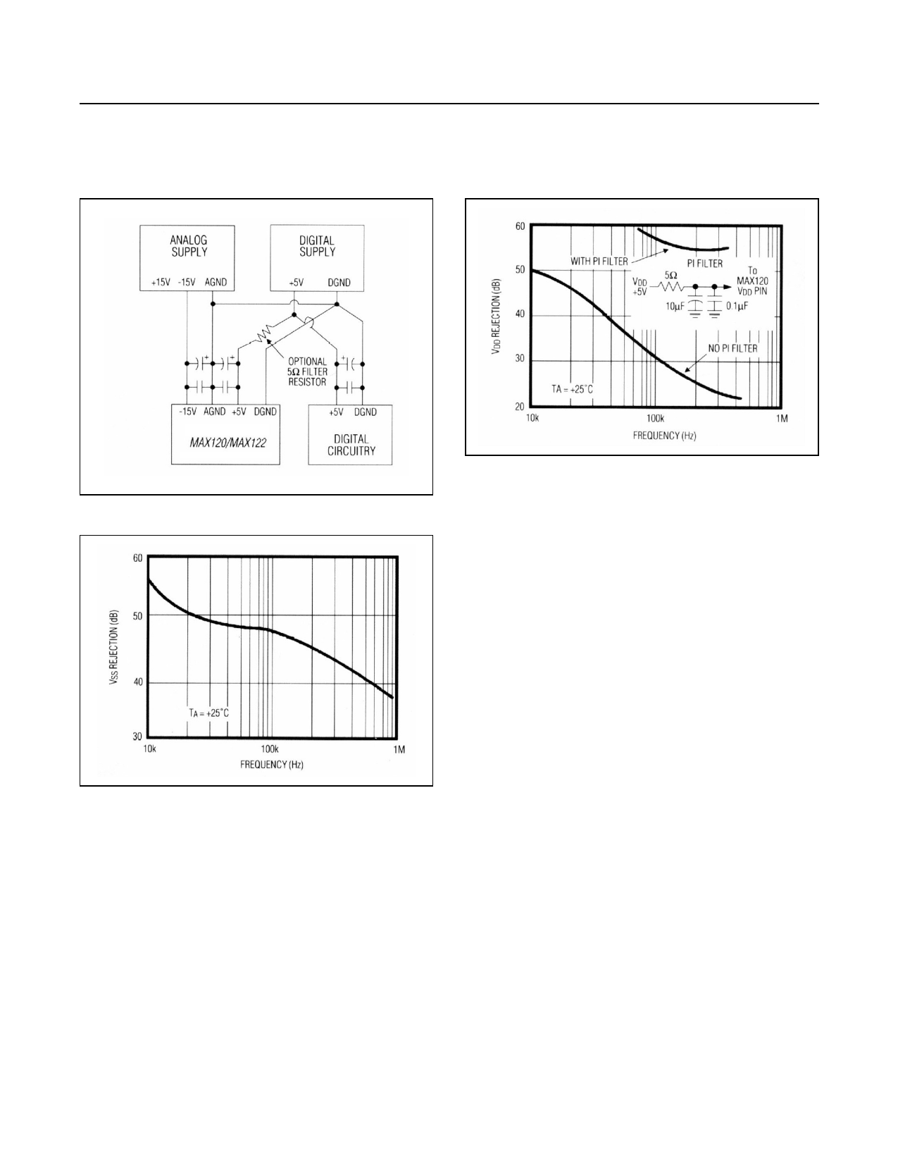
Figure 14. Power-Supply Grounding
Figure 15. VSS Power-Supply Rejection vs. Frequency
Gain and Offset Adjustment
Figure 17 plots the bipolar input/output transfer func-
tion for the MAX120/MAX122. Code transitions occur
halfway between successive integer LSB values. Output
coding is two’s-complement binary with 1 LSB = 2.44mV
(10V/4096).
In applications where gain (full-scale range) adjustment
is required, Figure 18’s circuit can be used. If both offset
and gain (full-scale range) need adjustment, either of the
circuits in Figures 19 and 20 can be used. Offset should
be adjusted before gain for either of these circuits.
Figure 16. VDD Power-Supply Rejection vs. Frequency
To adjust bipolar offset with Figure 19’s circuit, apply +1/2
LSB (0.61mV) to the noninverting amplifier input and
adjust R4 for output-code flicker between 0000 and 0000
0000 0001. For full scale, apply FS - the output code flick-
ers between 0111 1111 1110 and 0111 1111 1111. There
may be some interaction between these adjustments. The
MAX120/MAX122 transfer function used in conjunction
with Figure 19’s circuit is the same as Figure 17, except
the full-scale range is reduced to 2.5V.
To adjust bipolar offset with Figure 20’s circuit, apply
-1/2 LSB (-1.22mV) at VIN and adjust R5 for output-code
flicker between 0000 0000 0000 and 0000 0000 0001. For
gain adjustment, apply -FS + ½ LSB (-4.9951V) at VIN
and adjust R1 so the output code flickers between 0111
1111 1110 and 0111 1111 1111. As with Figure 20’s circuit,
the offset and gain adjustments may interact. Figure 21
plots the transfer function for Figure 20’s circuit.
Dynamic Performance
High-speed sampling capability and 500ksps throughput
(333ksps for the MAX122) make the MAX120/MAX122
ideal for wideband-signal processing. To support these
and other related applications, fast fourier transform (FFT)
test techniques are used to guarantee the ADC’s dynamic
frequency response, distortion, and noise at the rated
throughput. Specifically, this involves applying a low-
distortion sine wave to the ADC input and recording the
digital conversion results for a specified time. The data is
then analyzed using an FFT algorithm, which determines
its spectral content.
www.maximintegrated.com
Maxim Integrated │ 11
Share Link: 