LIS3L02DQ 데이터 시트보기 (PDF) - STMicroelectronics
부품명
상세내역
일치하는 목록
LIS3L02DQ Datasheet PDF : 19 Pages
| |||
LIS3L02DQ
CS is the Serial Port Enable and it is controlled by the SPI master. It goes low at the start of the transmis-
sion and goes back high at the end. SPC is the Serial Port Clock and it is controlled by the SPI master. It
is stopped high when CS is high (no transmission). SPDI and SPDO are respectively the Serial Port Data
Input and Output. Those lines are driven at the falling edge of SPC and should be captured at the rising
edge of SPC.
Both the Read Register and Write Register commands are completed in 16 clocks pulses. Bit duration is
the time between two falling edges of SPC. The first bit (bit 0) starts at the first falling edge of SPC after
the falling edge of CS while the last bit (bit 15) starts at the last falling edge of SPC just before the rising
edge of CS.
– bit 0: RW bit. When 0, the data DI(7:0) is written into the device. When 1, the data DO(7:0) from the
device is read. In latter case, the chip will drive SPDO at the start of bit 8.
– bit 1-7: address AD(6:0). This is the address field of the indexed register.
– bit 8-15: data DI(7:0) (write mode). This is the data that will be written into the device (MSb first).
– bit 8-15: data DO(7:0) (read mode). This is the data that will be read from the device (MSb first).
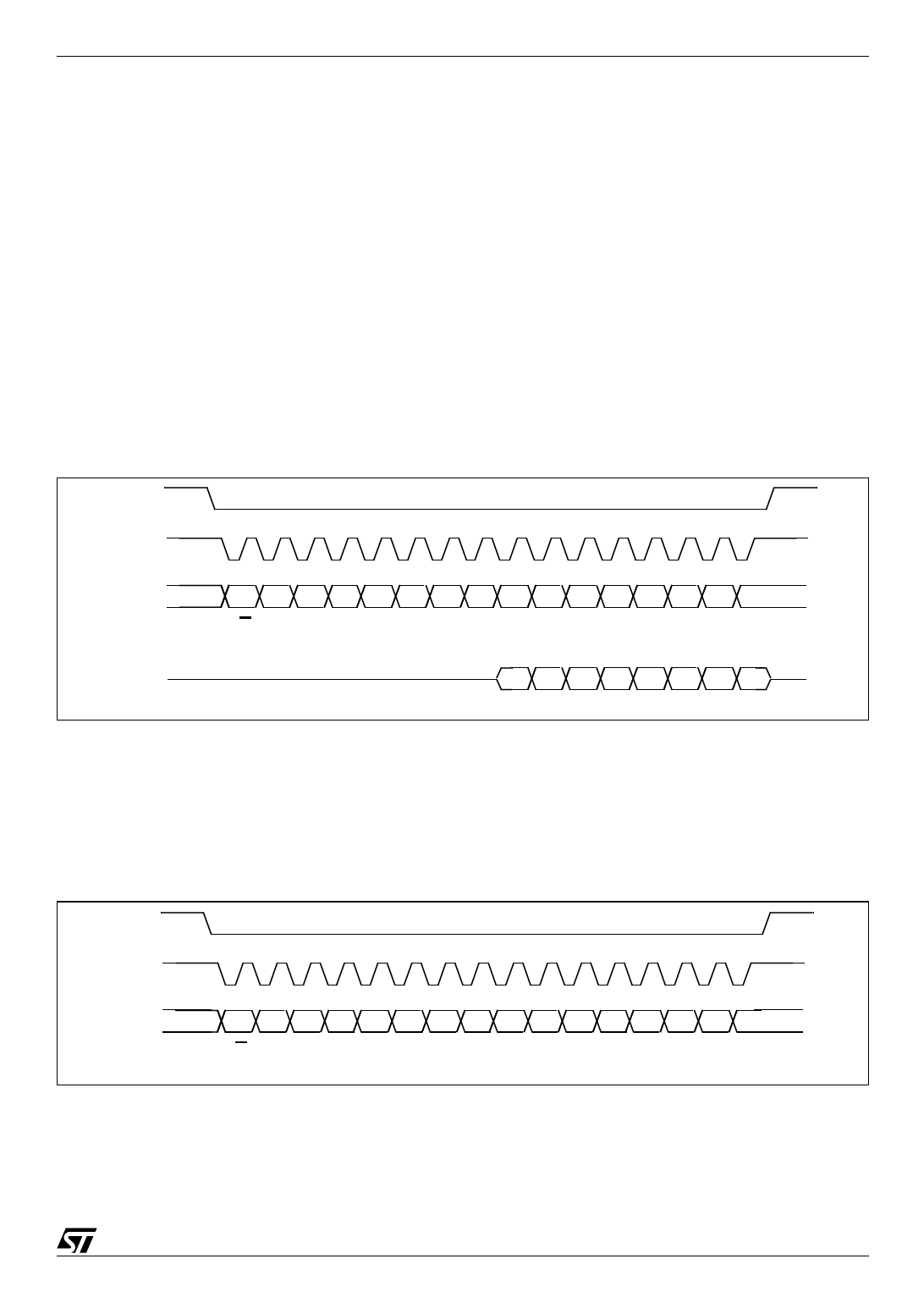
4.2.2 SPI Read
Figure 6. SPI Read protocol
CS
SPC
SPDI
RW
AD6 AD5 AD4 AD3 AD2 AD1 AD0
SPDO
DO7 DO6 DO5 DO4 DO3 DO2 DO1 DO0
The SPI Read command consists is performed with 16 clocks pulses:
– bit 0: READ bit. The value is 1.
– bit 1-7: address AD(6:0). This is the address field of the indexed register.
– bit 8-15: data DO(7:0) (read mode). This is the data that will be read from the device (MSb first).
4.2.3 SPI Write
Figure 7. SPI Write protocol
CS
SPC
SPDI
RW
DI7 DI6 DI5 DI4 DI3 DI2 DI1 DI0
AD6 AD5 AD4 AD3 AD2 AD1 AD0
The SPI Write command consists is performed with 16 clocks pulses.
– bit 0: WRITE bit. The value is 0.
– bit 1-7: address AD(3:0). This is the address field of the indexed register.
– bit 8-15: data DI(7:0) (write mode). This is the data that will be written inside the device (MSb first).
9/19
Share Link: 