LDA111 데이터 시트보기 (PDF) - IXYS CORPORATION
부품명
상세내역
일치하는 목록
LDA111 Datasheet PDF : 6 Pages
| |||
INTEGRATED CIRCUITS DIVISION
LDA111
Absolute Maximum Ratings @ 25ºC
Parameter
Breakdown Voltage
Reverse Input Voltage
Input Control Current
Peak (10ms)
Power Dissipation
Input Power Dissipation 1
Phototransistor 2
Isolation Voltage, Input to Output
Operational Temperature
Storage Temperature
1 Derate linearly 1.33mW / °C
2 Derate linearly 2mW / °C
Ratings
30
5
100
1
150
150
3750
-40 to +85
-40 to +125
Units
VP
V
mA
A
mW
Vrms
°C
°C
Absolute Maximum Ratings are stress ratings. Stresses in
excess of these ratings can cause permanent damage to
the device. Functional operation of the device at conditions
beyond those indicated in the operational sections of this
data sheet is not implied.
Electrical Characteristics @ 25ºC
Parameter
Output Characteristics
Phototransistor Breakdown Voltage
Phototransistor Dark Current
Saturation Voltage
Current Transfer Ratio
Output Capacitance
Input Characteristics
Input Control Current
Input Voltage Drop
Reverse Input Current
Common Characteristics
Capacitance, Input to Output
Conditions
Symbol Min Typ Max Units
IC = 100µA
BVCEO
30
85
-
V
VCEO = 5V, IF = 0mA
ICEO
-
50
500
nA
IC = 3mA, IF = 1mA
VCE(sat)
-
-
1
V
IF = 1mA, VCE = 2V
CTR 300 8500 30000 %
25V, f =1MHz
COUT
-
3
-
pF
IC = 3mA, VCE = 2V
IF
-
0.07
1
mA
IF = 5mA
VF
0.9
1.2
1.4
V
VR = 5V
IR
-
-
10
µA
-
CI/O
-
3
-
pF
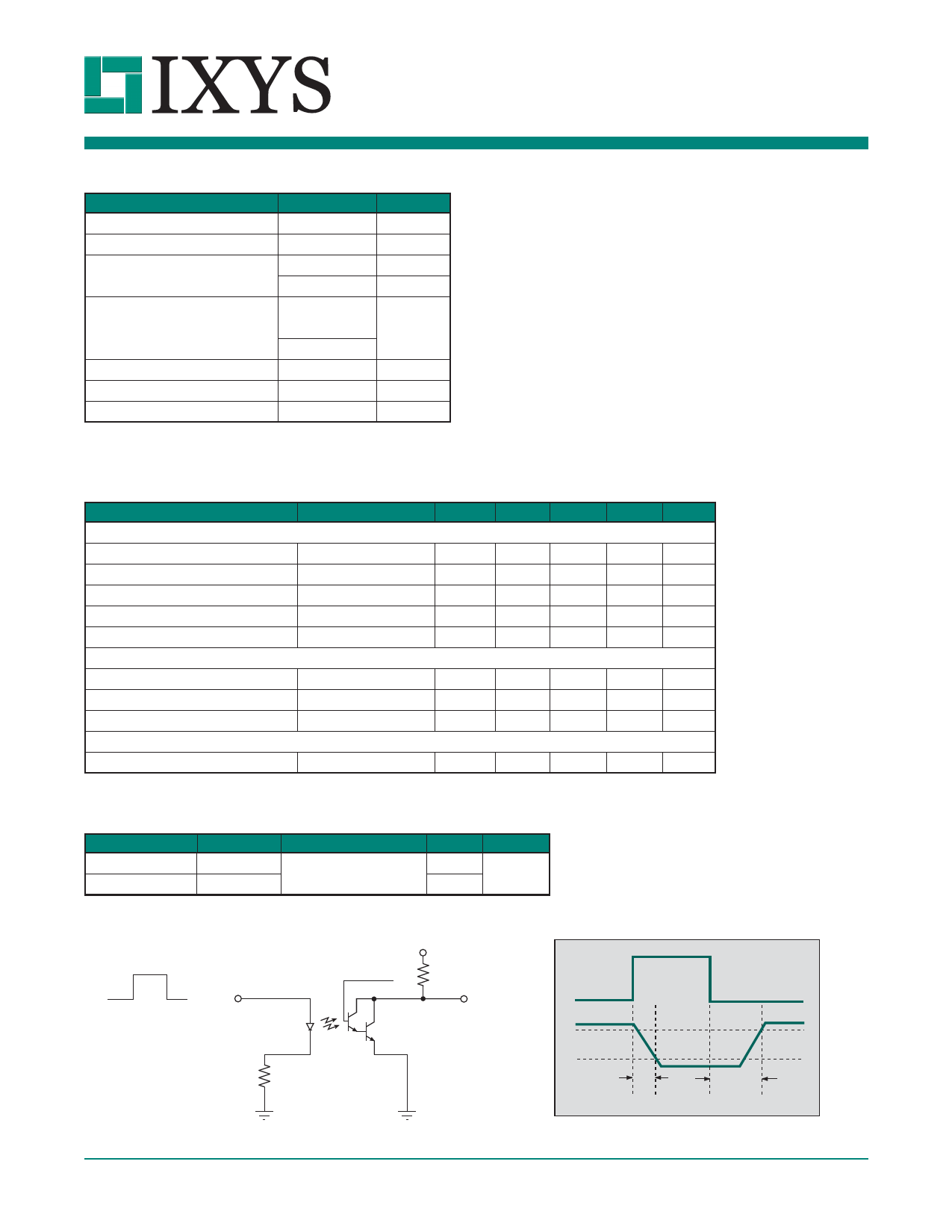
Switching Characteristics @ 25ºC
Characteristic
Turn-On Time
Turn-Off Time
Symbol
Test Condition
Typ
ton
toff
8
VCC=5V, IF=1mA, RL=500
345
Units
s
Switching Time Test Circuit
VCC
IF
Pulse Width=5ms
Duty Cycle=1%
RL
VCE
IF
VCE
90%
10%
t on
t off
2
www.ixysic.com
R06
Share Link: 