LC865612 데이터 시트보기 (PDF) - SANYO -> Panasonic
부품명
상세내역
일치하는 목록
LC865612 Datasheet PDF : 21 Pages
| |||
LC86E5632
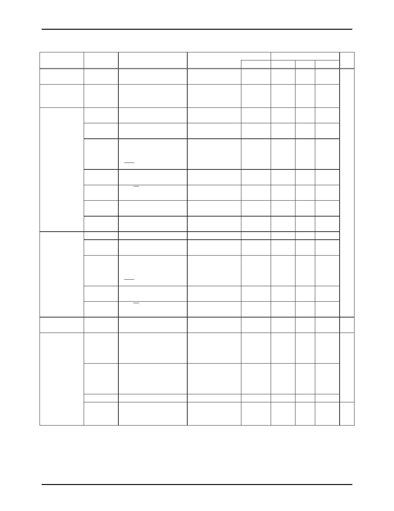
2. Recommended Operating Range at Ta=+10°C to +40°C, VSS=0V
Parameter
Operating
Supply voltage
Hold voltage
Symbol
VDD(1)
VHD
Input high
voltage
VIH(1)
VIH(2)
VIH(3)
Input low
voltage
VIH(4)
VIH(5)
VIH(6)
VIH(7)
VIL(1)
VIL(2)
VIL(3)
VIL(4)
VIL(5)
Operation
cycle time
Oscillation
frequency
range
(Note 1)
tCYC
FmCF(1)
FmCF(2)
FmRC
FsXtal
Pins
VDD
VDD
Port 0
(Schmitt)
•Ports 1,2
•Ports 72,73 (Schmitt)
•Port 70
(Port input/interrupt)
•Port 71
• RES
(Schmitt)
Port 70
(Watchdog timer)
•Port 74
•Port 8
Ports 3,4,5 of
CMOS output (Schmitt)
Ports 3,4,5 of open drain
output
(Schmitt)
Port 0
(Schmitt)
•Ports 1,2,3,4,5
•Ports 72,73 (Schmitt)
•Port 70
(Port input/interrupt)
•Port 71
• RES
(Schmitt)
Port 70
(Watchdog timer)
•Port 74
•Port 8
Conditions
VDD[V]
Ratings
unit
min. typ. max.
0.98µs ≤ tCYC
tCYC ≤ 400µs
4.5
6.0 V
RAMs and the
2.0
6.0
registers hold voltage
at HOLD mode.
Output disable
4.5 to 6.0 0.4VDD
VDD
+0.9
Output disable
4.5 to 6.0 0.75VDD
VDD
Output N-channel
Tr. OFF
4.5 to 6.0 0.75VDD
VDD
Output N-channel
Tr. OFF
Output N-channel
Tr. OFF
Output disable
Output disable
Output disable
Output disable
N-channel Tr.OFF
4.5 to 6.0 0.9VDD
4.5 to 6.0 0.75VDD
4.5 to 6.0 0.75VDD
4.5 to 6.0 0.75VDD
4.5 to 6.0 VSS
4.5 to 6.0 VSS
4.5 to 6.0 VSS
VDD
VDD
VDD
13.5
0.2VDD
0.25VDD
0.25VDD
N-channel Tr.OFF
N-channel Tr.OFF
4.5 to 6.0 VSS
4.5 to 6.0 VSS
4.5 to 6.0 0.98
0. 8VDD
-1.0
0.25VDD
400 µs
CF1, CF2
CF1, CF2
XT1, XT2
•6MHz
(ceramic resonator
oscillation)
•Refer to figure 1
•1.5MHz
(ceramic resonator
oscillation)
•Refer to figure 1
RC oscillation
•32.768kHz
(crystal oscillation)
•Refer to figure 2
Continue.
4.5 to 6.0
4.5 to 6.0
4.5 to 6.0
4.5 to 6.0
6
MHz
1.5
0.3
0.8
3.0
32.768
kHz
No.6744-11/21
Share Link: 