LB1964 데이터 시트보기 (PDF) - SANYO -> Panasonic
부품명
상세내역
일치하는 목록
LB1964 Datasheet PDF : 4 Pages
| |||
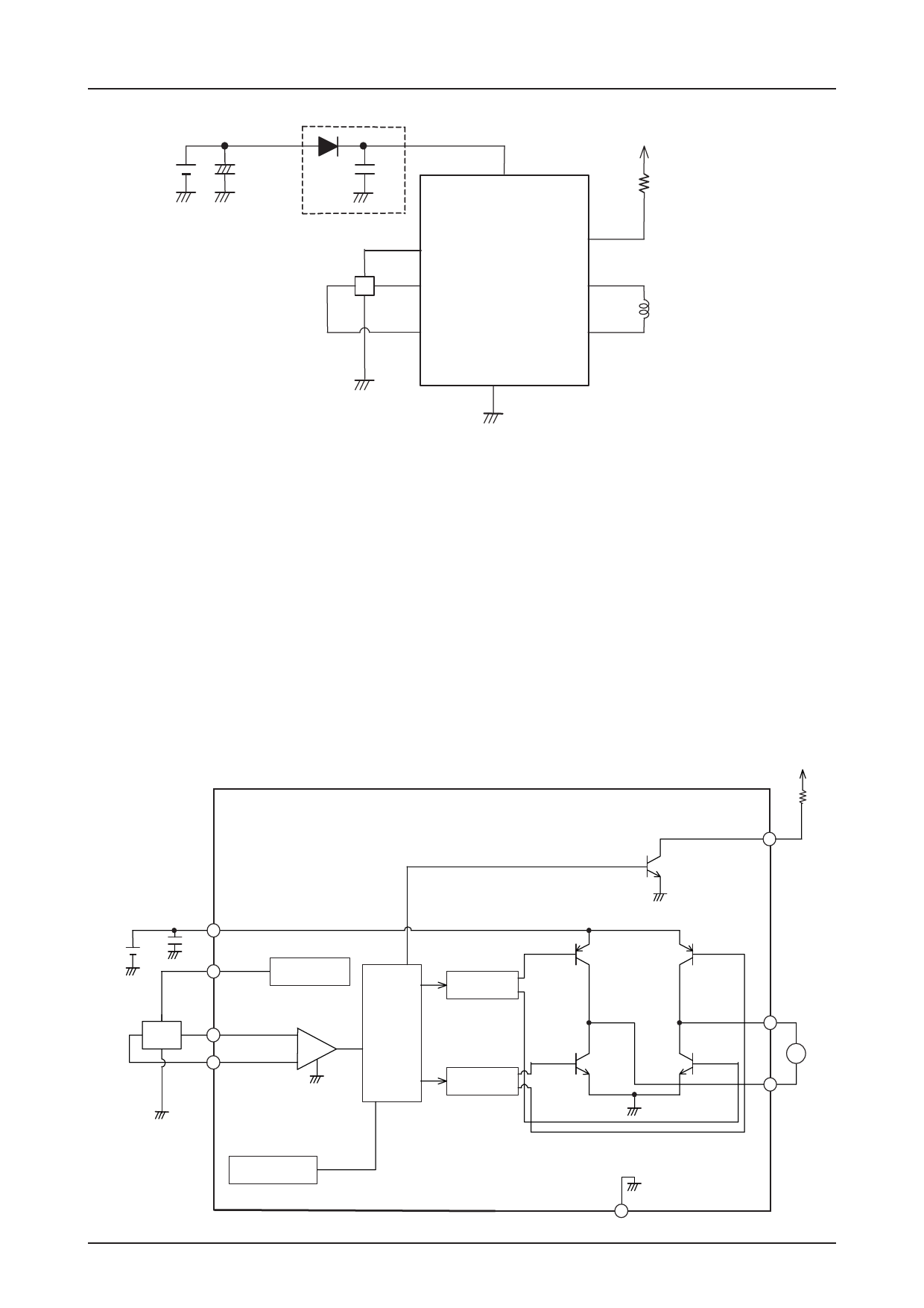
Sample Application Circuit
LB1964T
Di
Cr
∗1
∗2
H
∗3
VCC
FG
HB
IN–
OUT1
IN+
OUT2
GND
*1 When a diode is used to protect the IC from destruction in case of reverse connection, the capacitor Cr
must be inserted to provide a regenerative current route. Similarly, a capacitor is needed in the power
supply line, even if no diode is used.
*2 The Hall element is supplied with a constant-voltage bias of approx. 1.27V from the HB pin. This
ensures stable output with good temperature characteristics from the Hall element. Because the
LB1964T incorporates a Hall amplifier with low offset, it provides coil output with a stable duty.
*3 The Hall amplifier does not have a hysteresis characteristic. The OUT1 and IN– pins are at the same
phase, and by arranging the two pins next to each other, chatter during phase switching is prevented.
However, if the wiring leading to the IN– pin is long, some noise interference may occur. In such a
case, the following steps should be considered:
(1) Arrange parts layout with priority to proximity of Hall element and IC, to allow short Hall element
output wiring.
(2) Insert a resistor of about 10 to 100 kΩ between OUT1 and IN– to create a hysteresis characteristic.
Block Diagram
FG
VCC
HB
IN+
HALL
IN–
Constant voltage
circuit
Control
circuit
Delay circuit
Delay circuit
Thermal protection
circuit
GND
OUT2
M
OUT1
No. 6188-3/4
Share Link: 