L4955 데이터 시트보기 (PDF) - STMicroelectronics
부품명
상세내역
일치하는 목록
L4955 Datasheet PDF : 14 Pages
| |||
L4955
L4955V3.3
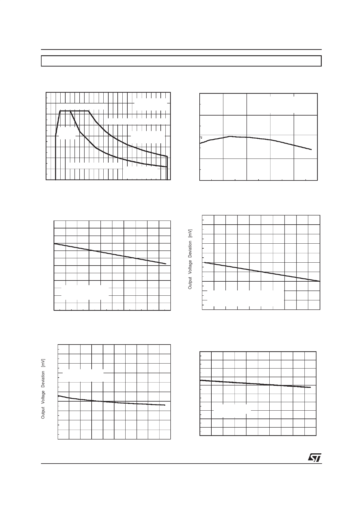
Figure 23: DC operating area.
Output Current [A]
8
7
Current Lim itation
Vout = 3.3V
Tj = 125°C
6
5
Rdson
4
lim it
Power Dissipation Lim it
Tc = 25°C
P d m ax = 4 0W
3
Figure 24: Output Voltage Stability vs. Junction
Temperature.
Vo ut [V ]
3 .4
V in = 5V
Iout = 10mA
3 .35
3 .3
2
DC O perating Area
1
T c = 7 0° C
P d m ax = 2 2W
0
3 4.5 6 7.5 9 10.5 12 13.5 15 16.5 18 19.5 21 22.5
Input Voltage [V]
Figure 25: Quiescent Current vs. Temperature.
3 .25
3 .2
-4 0
0
40
80
Tj [°C]
Figure 26: Load Regulation
120
160
Iq [m A]
5
3
4
2 .7 5
2 .5
3
2 .2 5
2
2
1
1 .7 5
0
1 .5
1 .2 5
-1
1
-2
0 .7 5
0 .5
0 .2 5
V in=5V
Iout = 10mA to 5A
-3 Vin=5V
-4 Tj = 25 °C
(Pulsed tecnique has been used)
0
-5
-40 -20 0 20 40 60 80 100 120 140 160
0
1
2
3
4
5
T j [°C ]
Iout [A]
Figure 27: Line regulation vs. Junction Tempera-
ture.
5
4.5
4
3.5
4.5 V < V in < 12 V
Io u t = 1 0 m A
3
2.5
2
1.5
1
0.5
0
-40 -20 0 20 40 60 80 100 120 140 160
Tj [°C]
10/14
Figure 28: MaximumOutput Current vs.Junction
Temperaturewith internalcurrent limiting
O utput Current [A]
10
9
8
7
6
5
4
(Vin-Vout) > 2V
3
pin 2 = GND
2
1
0
-40 -20 0 20 40 60 80 100 120 140 160
Tj [°C]
*Pulsed tecnique has been used
Share Link: 