TDA8133_09 데이터 시트보기 (PDF) - STMicroelectronics
부품명
상세내역
일치하는 목록
TDA8133_09 Datasheet PDF : 14 Pages
| |||
TDA8133
Power dissipation and layout indications
5
Power dissipation and layout indications
The power is mainly dissipated by the two device buffers. It can be calculated by the
equation:
P = (VIN1-VO1) x IO1 + (VIN2-VO2) x IO2
The following table lists the different RthJA values of these packages with or without a heat
sink and the corresponding maximum power dissipation assuming:
● Maximum ambient temperature = 70° C
● Maximum junction temperature = 140° C
Table 5. Power dissipation
Device
Heat Sink
RthJA in °C/W
PMAX in W
No
50
1.4
TDA8133
Yes
t(s) No
TDA8133D
Yes
20
56 to 40
32
3.5
1.25 to 1.75
2.2
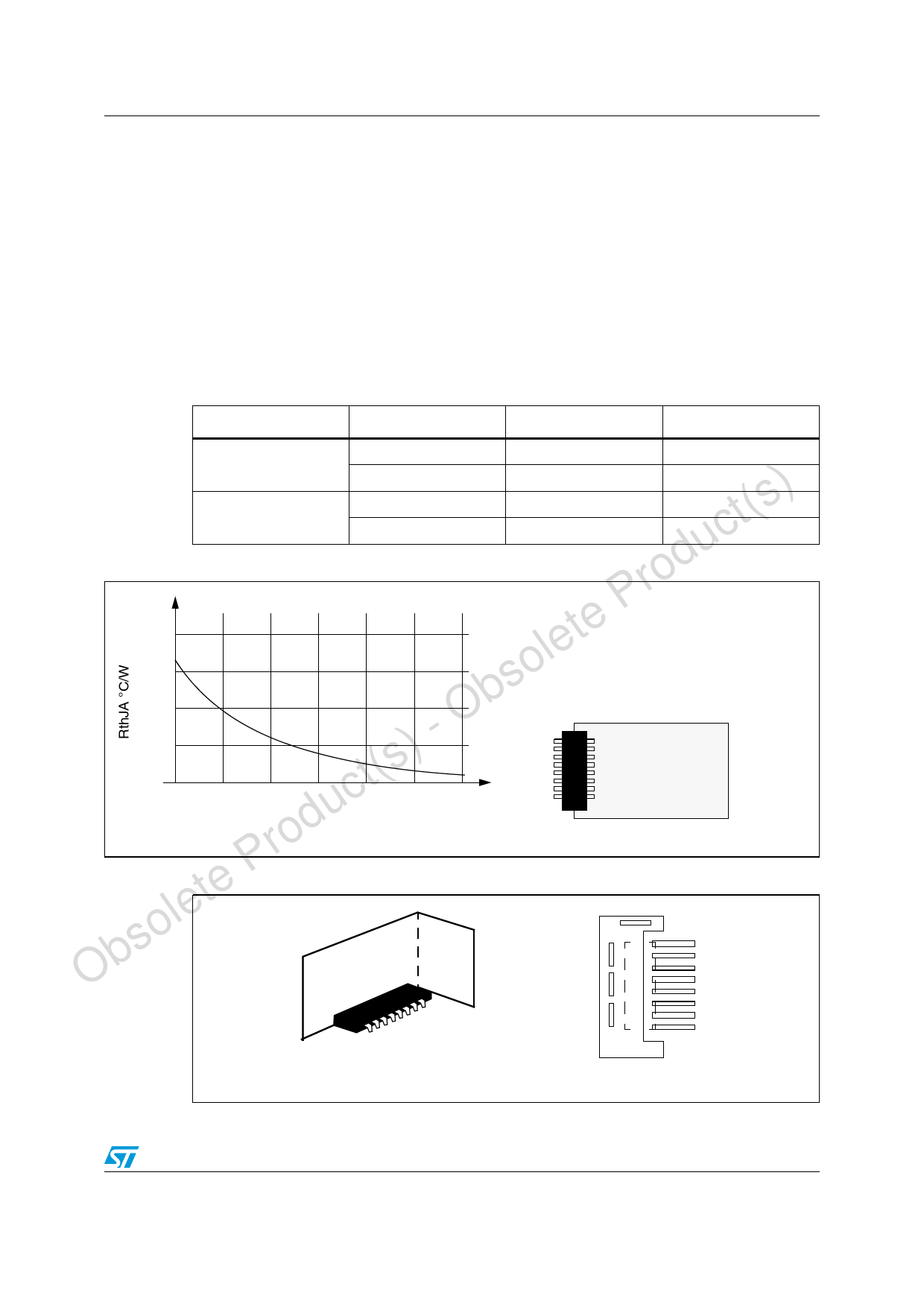
duc Figure 8. Thermal resistance (junction-to-ambient) for DIP16 package without heatsink
Pro To optimize the thermal conductivity of the copper
te 60
layer and the exchanges with the air, the solder
must cover the maximum amount of this area
ole 55
s Test board with
b 50
“on board” square heat sink area
- O 45
t(s) 40
c 0
2
4
6
8
10 12
u Copper area (cm²) (35 µm plus solder) board is face-down
Obsolete Prod Figure 9. Metal plate mounted near the TDA8133D for heatsinking
Top View
Bottom View
9/14
Share Link: 