TDA8132 데이터 시트보기 (PDF) - STMicroelectronics
부품명
상세내역
일치하는 목록
TDA8132 Datasheet PDF : 6 Pages
| |||
TDA8132
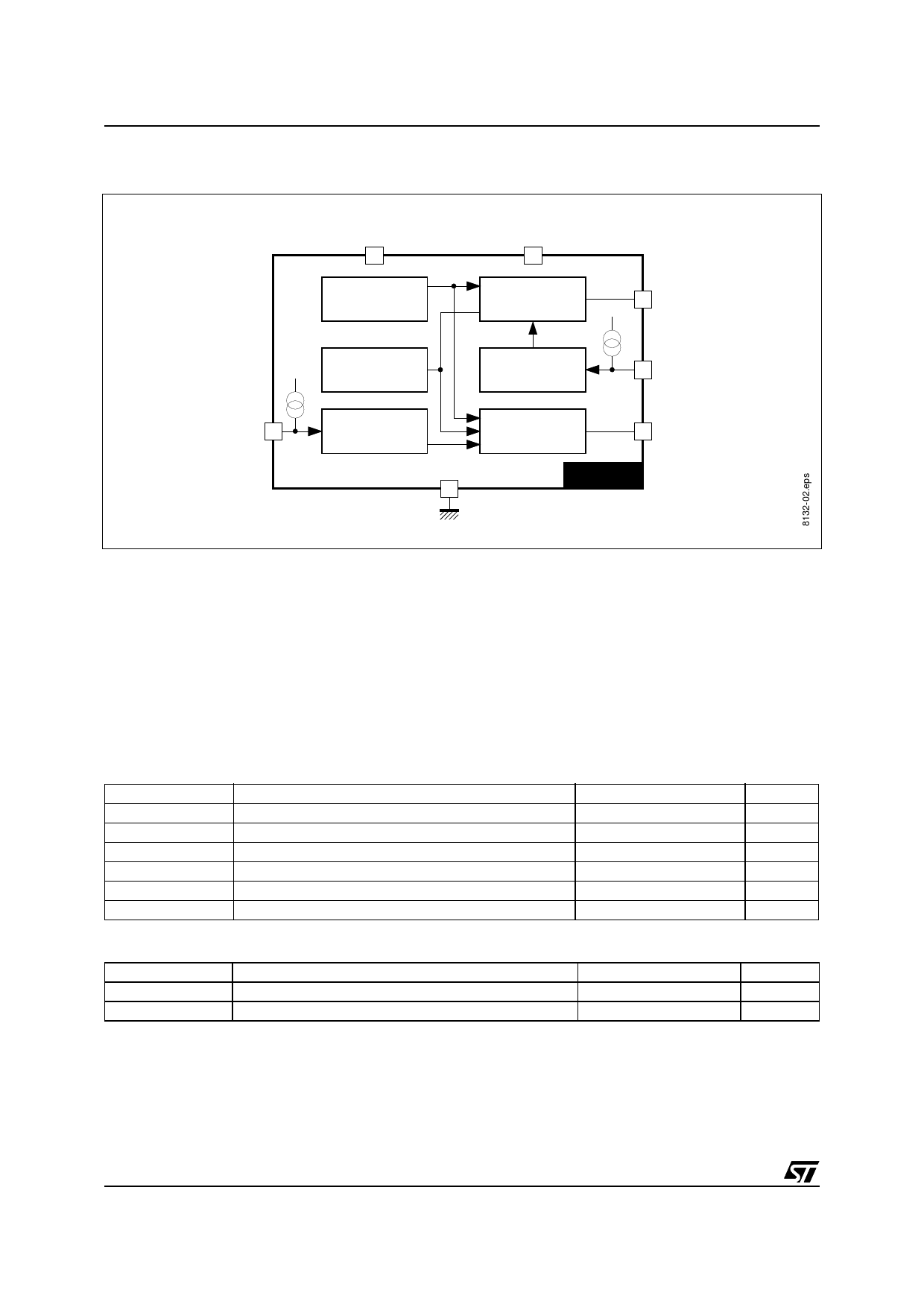
Figure 2. Block Diagram
INPUT 1
1
REFERENCE
INPUT 2
2
OUTPUT 1
7 OUTPUT 1
DISABLE 3
PROTECTION
DISABLE
5 DISABLE
DISABLE
4
OUTPUT 2
6 OUTPUT 2
TDA8132
CIRCUIT DESCRIPTION
The TDA8132 is a dual voltage regulator with sep-
arate Disable for each output.
The two regulation parts are supplied from one
voltage reference circuit trimmed by zener zap
during EWS test.
Since the supply voltage of this last is connected
at Pin 1 (VIN1), the regulator 2 will not work if Pin 1
is not supplied.
ABSOLUTE MAXIMUM RATINGS
Symbol
VIN
VDIS
IO1, 2
Pt
TSTG
TJ
Parameter
DC Input Voltage Pin 1
Disable Input Voltage Pin 3-5
Output Currents
Power Dissipation
Storage Temperature
unction Temperature
The outputs stage have been realized in darlington
configuration with a drop typical 1.2V.
For each output a disable circuit switches-off this
output if a voltage lower than 0.8V is applied at
corresponding Pin (Pin 3 for output 2, Pin 5 for out-
put 1).
Value
20
20
Internally Limited
Internally Limited
- 65 to + 150
0 to + 150
Unit
V
V
°C
°C
THERMAL DATA
Symbol
RTH(j-c)
TJ
Parameter
Thermal Resistance Junction-case
Recommended Junction Temperature
Max.
Max.
Value
3
130
Unit
°C/W
°C
2/5
1
Share Link: 