KC2016B-C1 데이터 시트보기 (PDF) - Kyocera Kinseki Corpotation
부품명
상세내역
일치하는 목록
KC2016B-C1 Datasheet PDF : 1 Pages
| |||
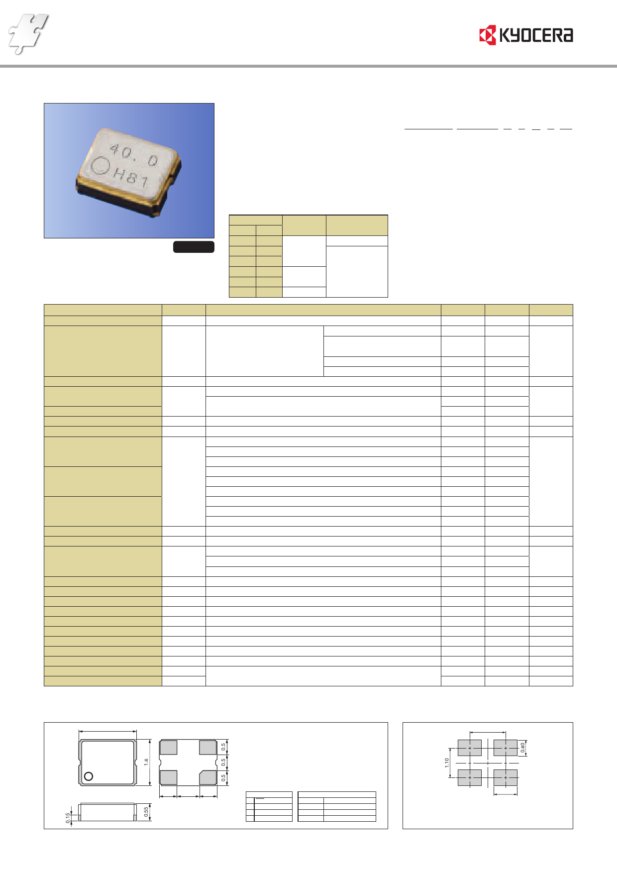
Clock Oscillators Surface Mount Type
KC2016B-C1 Series
CMOS/ 1.8V to 3.3V/ 2.0×1.6mm
Specifications
RoHS Compliant
Features
• Ultra Miniature ceramic package
2.0 (L) ×1.6 (W) ×0.55 (H) mm (Typ.)
• Highly reliable with seam welding
• CMOS output
• Supply voltage Vcc=1.8V/ 2.5V/ 3.3V
Wide operating voltage range 1.6 to 3.63V
• Low current consumption
Table 1
Freq. Tol. Operating
Code
× 10−6
Temperature
Range (°C)
Note
0 ± 50
Standard speci cations
S ± 30 −10 to +70
U ± 25
Please contact
F
G
±100
± 50
−40 to +85
us for available
frequencies.
6 ± 50 −40 to +105
How to Order
KC2016B 40.0000 C 1 □ E 00
①
② ③④⑤⑥⑦
① Series
② Output Frequency
③ Output Type (CMOS)
④ Supply Voltage (1.8V, 2.5V, 3.3V Compatible)
⑤ Frequency Tolerance (See Table 1)
⑥ Symmetry/ INH Function
(45/ 55%, Stand-by)
⑦ Individual Speci cation
(STD Speci cation is “00”)
Packaging (Tape & Reel 2000 pcs./ reel)
Item
Output Frequency Range
Frequency Tolerance
Storage Temperature Range
Operating Temperature Range
Symbol
fo
f_tol
T_stg
T_use
Conditions
Initial tolerance, Operating tem- Op. Temp.: −40 to +85°C
perature range, Rated power Op. Temp.: −10 to +70°C/
supply voltage change, Aging −40 to +85°C/ −40 to +105°C
(1 year @25°C), Shock and vi- Op. Temp.: −10 to +70°C
bration
Op. Temp.: −10 to +70°C
Standard Speci cations
Extend (Option)
Max. Supply Voltage
Supply Voltage
Current Consumption
(Maximum Loaded/ 1.6≤VCC≤2.0V)
Current Consumption
(Maximum Loaded/ 2.0<VCC≤2.8V)
Current Consumption
(Maximum Loaded/ 2.8<VCC≤3.63V)
Stand-by Current
Symmetry
Rise/ Fall Time
(10% VCC to 90% VCC Maximum Loaded)
Low Level Output Voltage
High Level Output Voltage
CMOS Load
Input Voltage Range
Low Level Input Voltage
High Level Input Voltage
Disable Time
Enable Time
Start-up Time
1 Sigma Jitter
Peak to Peak Jitter
—
VCC
ICC
I_std
SYM
tr/ tf
VOL
VOH
L_CMOS
VIN
VIL
VIH
t_dis
t_ena
t_str
JSigma
JPK-PK
1.5≤fo≤24MHz
24<fo≤40MHz
40<fo≤50MHz
1.5≤fo≤24MHz
24<fo≤40MHz
40<fo≤50MHz
1.5≤fo≤24MHz
24<fo≤40MHz
40<fo≤50MHz
@50% VCC
1.6≤VCC≤2.0V
2.0<VCC≤2.8V
2.8<VCC≤3.63V
IOL=4mA
IOH=−4mA
CMOS Output
@Minimum operating voltage to be 0 sec.
Measured with Wavecrest SIA-3000
Note: All electrical characteristics are defined at the maximum load and operating temperature range.
Please contact us for inquiry about operating temperature range, available frequencies and other conditions.
Min.
1.5
−100
−50
−30
−25
−55
−10
−40
−40
−0.6
+1.6
—
—
—
—
—
—
—
—
—
—
45
—
—
—
—
90% VCC
—
0
—
70% VCC
—
—
—
—
—
Max.
50
+100
+50
+30
+25
+125
+70
+85
+105
+6.0
+3.63
2.5
3.5
4.5
3.0
4.5
5.0
3.5
5.0
6.0
10
55
6.5
5.0
4.5
10% VCC
—
15
VCC
30% VCC
—
100
5
10
8
80
Units
MHz
×10−6
°C
°C
V
V
mA
μA
%
ns
V
V
pF
V
V
V
ns
ms
ms
ps
ps
Dimensions
(Unit: mm) Recommended Land Pattern (Unit: mm)
2.0
1.40
#3 #4
#2 #1
Plating: NiAu
Tolerance: r0.1
0.6 0.7 0.6
Pad Connections
#1 INH
#2 Case GND
#3 Output
#4 VCC
INH Function
Pad1
Pad3 (Output)
Open
Active
"H" Level
Active
"L" Level High Z (No-Oscillation)
0.90
Note: A capacitor of value 0.01PF between VCC
and GND is recommended.
As of March 2018
Share Link: 