KA3032 데이터 시트보기 (PDF) - Fairchild Semiconductor
부품명
상세내역
일치하는 목록
KA3032 Datasheet PDF : 24 Pages
| |||
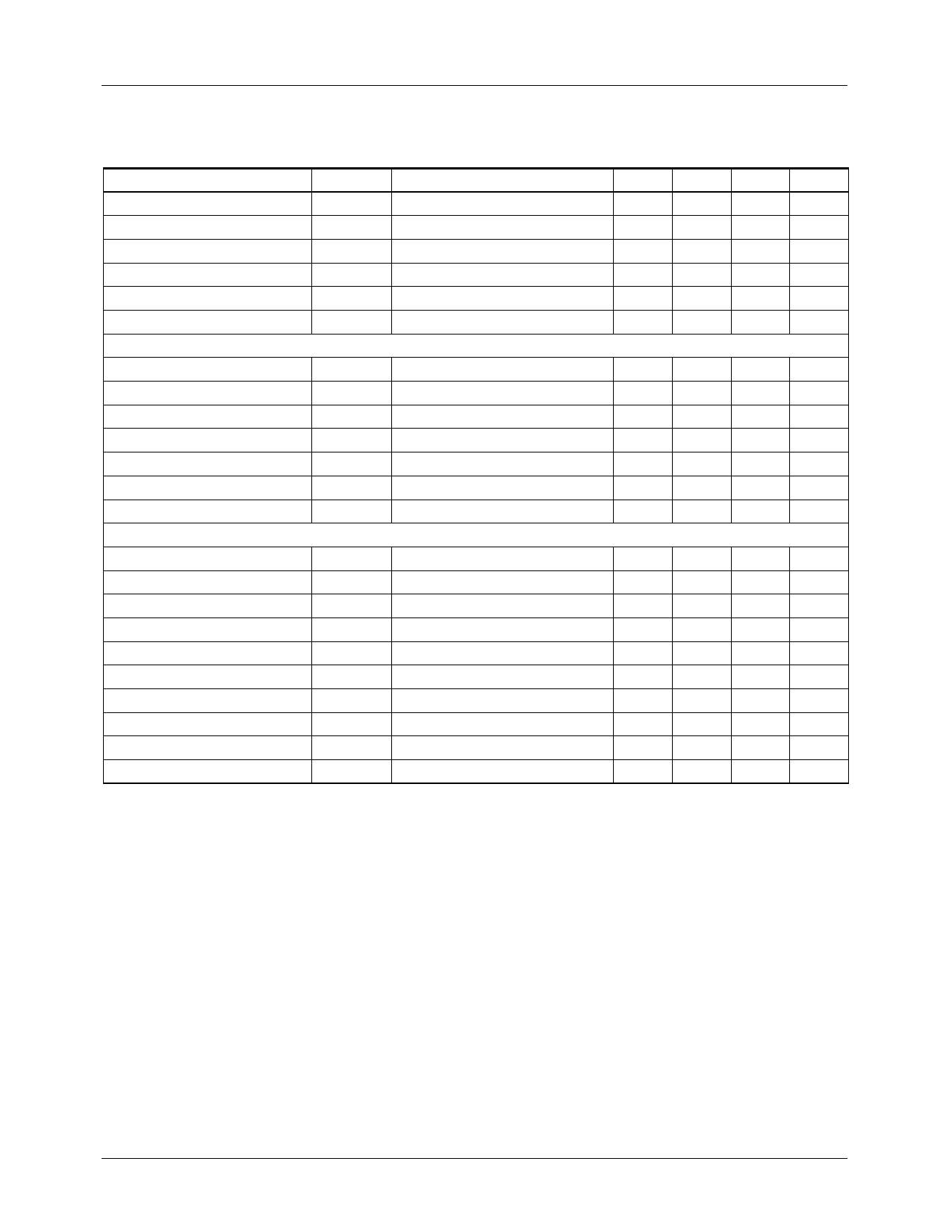
KA3032
Electrical Characteristics
(SVCC=PVCC1=PVCC2=8V, Ta=25°C, unless otherwise specified)
Parameter
Symbol
Conditions
Quiescent circuit current
ICC
under no-load
All mute on current
IMUTE ALL Pin 46=GND
All mute on voltage
VMON ALL Pin 46=Variation
All mute off voltage
VMOFF ALL Pin 46=Variation
CH mute on voltage
VMON CH Pin 22, 23, 24=Variation
CH mute off voltage
VMOFF ALL Pin 22, 23, 24=Variation
DRIVER PART (RL=8Ω)
Input offset voltage
VIO
-
Output offset voltage
Maximum output voltage 1
VOO
VOM1
VIN=2.5V
VCC=8V, RL=8Ω
Maximum output voltage 2
VOM2 VCC=13V, RL=24Ω
Closed-loop voltage gain
AVF
VIN=0.1VRMS
Ripple rejection ratio
RR
VIN=0.1VRMS, f=120kHz
Slew rate
SR
Square, Vout=2Vp-p, f=120kHz
NORMAL OPAMP PART
Input offset voltage
VOF1
-
Input bias current
IB1
-
High level output voltage
VOH1 RL=50Ω
Low level output voltage
VOL1 RL=50Ω
Output sink current
ISINK1 VIN=−75dB, f=1kHz
Output source current
ISOURCE1 VIN=−20dB, f=120kHz
Open loop voltage gain
GVO1 Square, Vout=2Vp-p, f=120kHz
Ripple rejection ratio
RR1 VIN=−20dB, f=1kHz
Slew rate
SR1
-
Common mode rejection ratio CMRR1
-
Min.
9
-
-
2
2
-
−20
−50
4.7
7
9
-
-
−10
-
6
-
10
10
-
-
-
-
Typ.
12
6
-
-
-
-
-
-
5.5
9
10.5
50
0.8
-
-
6.8
1.0
40
40
75
65
1
80
Max.
16
10
0.5
-
-
0.5
Units
mA
mA
V
V
V
V
+20 mV
+50 mV
-
V
-
V
12
dB
-
dB
-
V/µs
+10 mV
300 nA
-
V
1.8
V
-
mA
-
mA
-
dB
-
dB
-
V/µs
-
dB
11
Share Link: 