K4E641612C 데이터 시트보기 (PDF) - Samsung
부품명
상세내역
일치하는 목록
K4E641612C Datasheet PDF : 36 Pages
| |||
K4E661612C,K4E641612C
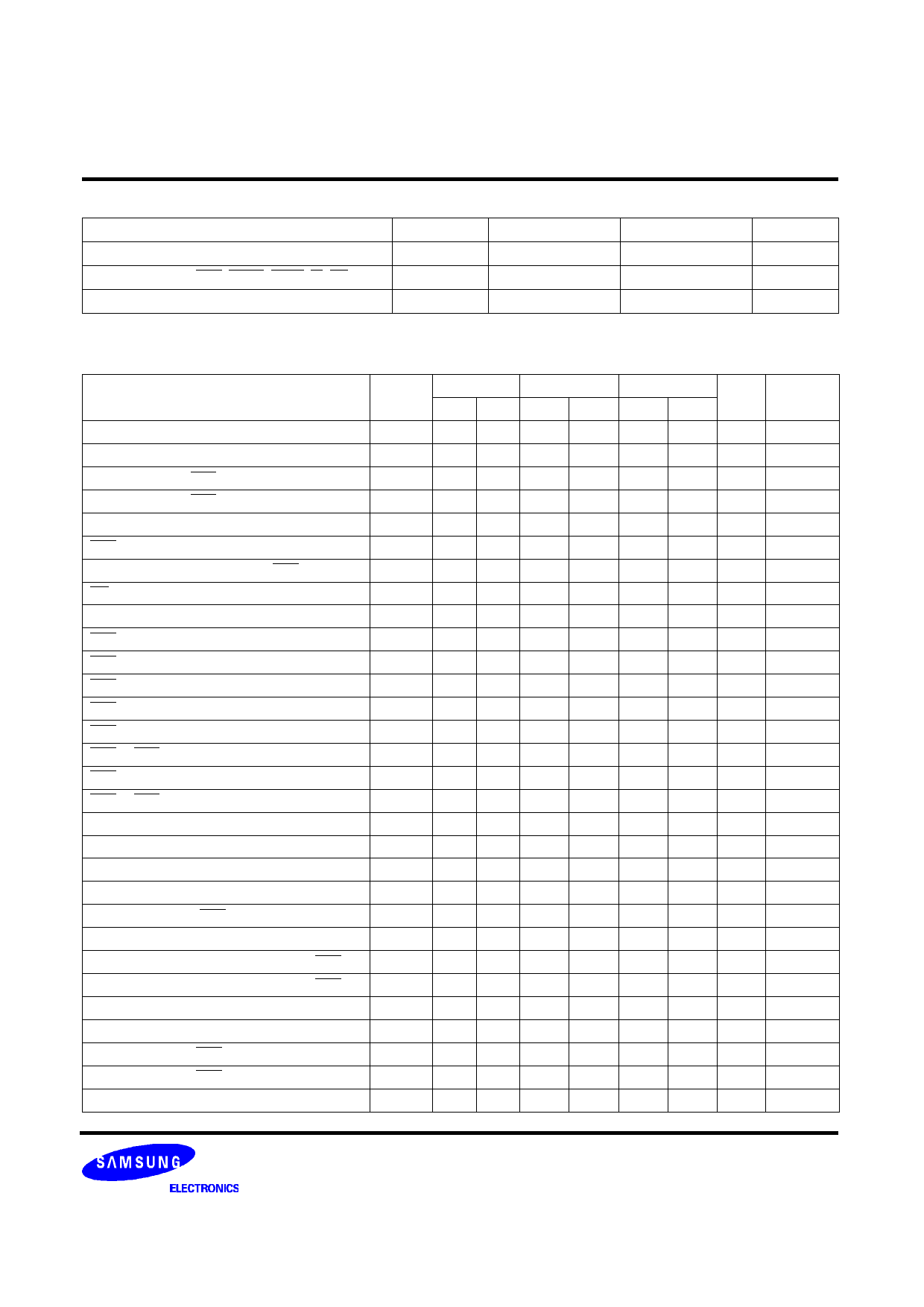
CAPACITANCE (TA=25°C, VCC=3.3V, f=1MHz)
Parameter
Symbol
Min
Input capacitance [A0 ~ A12]
CIN1
-
Input capacitance [RAS, UCAS, LCAS, W, OE]
CIN2
-
Output capacitance [DQ0 - DQ15]
CDQ
-
CMOS DRAM
Max
Units
5
pF
7
pF
7
pF
AC CHARACTERISTICS (0°C≤TA≤70°C, See note 2)
Test condition : VCC=3.3V±0.3V, Vih/Vil=2.2/0.7V, Voh/Vol=2.0/0.8V
Parameter
-45
Symbol
Min Max
Random read or write cycle time
tRC
74
Read-modify-write cycle time
Access time from RAS
tRWC
tRAC
101
45
Access time from CAS
tCAC
12
Access time from column address
CAS to output in Low-Z
Output buffer turn-off delay from CAS
tAA
tCLZ
tCEZ
23
3
3
13
OE to output in Low-Z
tOLZ
3
Transition time (rise and fall)
RAS precharge time
tT
1
50
tRP
25
RAS pulse width
tRAS
45 10K
RAS hold time
CAS hold time
CAS pulse width
tRSH
tCSH
tCAS
8
35
7
5K
RAS to CAS delay time
tRCD
11 33
RAS to column address delay time
CAS to RAS precharge time
Row address set-up time
tRAD
tCRP
tASR
9
22
5
0
Row address hold time
tRAH
7
Column address set-up time
Column address hold time
Column address to RAS lead time
tASC
0
tCAH
7
tRAL
23
Read command set-up time
tRCS
0
Read command hold time referenced to CAS
tRCH
0
Read command hold time referenced to RAS
tRRH
0
Write command hold time
tWCH
7
Write command pulse width
Write command to RAS lead time
Write command to CAS lead time
Data set-up time
tWP
6
tRWL
8
tCWL
7
tDS
0
-50
Min Max
84
113
50
13
25
3
3
13
3
1
50
30
50 10K
8
38
8
10K
11
37
9
25
5
0
7
0
7
25
0
0
0
7
7
8
7
0
-60
Min Max
104
138
60
15
30
3
3
13
3
1
50
40
60 10K
10
40
10 10K
14
45
12
30
5
0
10
0
10
30
0
0
0
10
10
10
10
0
Unit
s
ns
ns
ns
ns
ns
ns
ns
ns
ns
ns
ns
ns
ns
ns
ns
ns
ns
ns
ns
ns
ns
ns
ns
ns
ns
ns
ns
ns
ns
ns
Note
3,4,10
3,4,5
3,10
3
6,20
3
2
4
10
13
13
8
8
16
9,19
Share Link: 