IW4051B 데이터 시트보기 (PDF) - Unspecified
부품명
상세내역
일치하는 목록
IW4051B Datasheet PDF : 6 Pages
| |||
TECHNICAL DATA
IW4051B
Analog Multiplexer Demultiplexer
High-Performance Silicon-Gate CMOS
The IW4051B analog multiplexer/demultiplexer is digitally
controlled analog switches having low ON impedance and very low
OFF leakage current. Control of analog signals up to 20V peak-to-
peak can be achieved by digital signal amplitudes of 4.5 to 20V (if VCC
- GND = 3V, a VCC - VEE of up to 13 V can be controlled; for VCC -
VEE level differences above 13V a VCC - GND of at least 4.5V is
required).
These multiplexer circuits dissipate extremely low quiescent power
over the full VCC -GND and VCC - VEE supply-voltage ranges,
independent of the logic state of the control signals. When a logic
“1”is present at the ENABLE input terminal all channels are off.
The IW4051B is a single 8-channel multiplexer having three binary
control inputs, A,B and C, and an ENABLE input. The three binary
signals select 1 of 8 channels to be turned on, and connect one of the 8
inputs to the output.
• Operating Voltage Range: 3.0 to 18 V
• Maximum input current of 1 µA at 18 V over full package-
temperature range; 100 nA at 18 V and 25°C
• Noise margin (over full package temperature range):
1.0 V min @ 5.0 V supply
2.0 V min @ 10.0 V supply
2.5 V min @ 15.0 V supply
ORDERING INFORMATION
IW4051BN Plastic
IW4051BDW SOIC
TA = -55° to 125° C for all packages
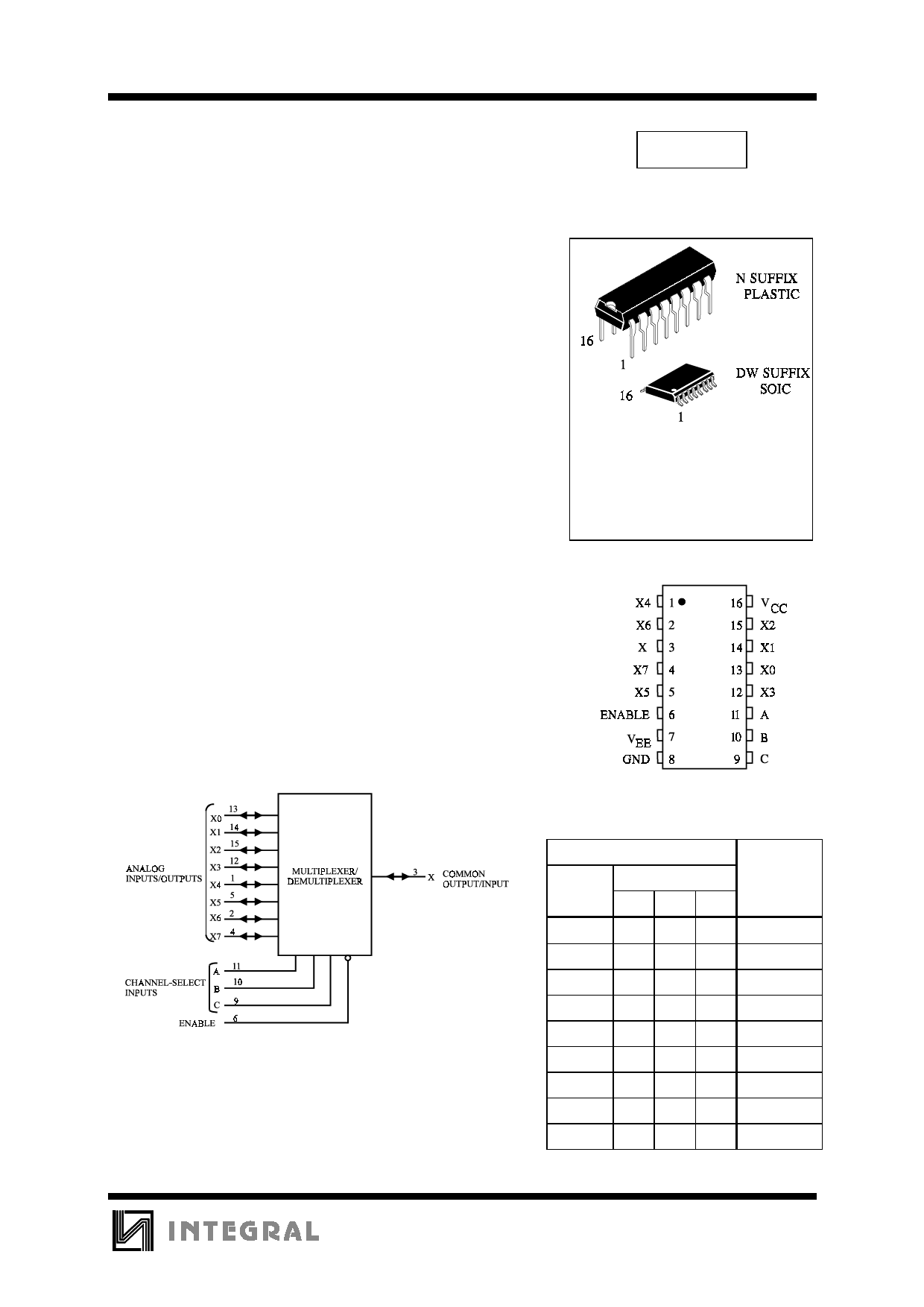
PIN ASSIGNMENT
LOGIC DIAGRAM
Single-Pole, 8-Position Plus Common Off
PIN 16 =VCC
PIN 7 = VEE
PIN 8 = GND
FUNCTION TABLE
Control Inputs
Enable
Select
CBA
L
LLL
L
LLH
L
LHL
L
LHH
L
HLL
L
HLH
L
HH L
L
HHH
H
XXX
X = don’t care
ON
Channels
X0
X1
X2
X3
X4
X5
X6
X7
None
97
Share Link: 