ISL97645(2006) 데이터 시트보기 (PDF) - Intersil
부품명
상세내역
일치하는 목록
ISL97645 Datasheet PDF : 14 Pages
| |||
ISL97645
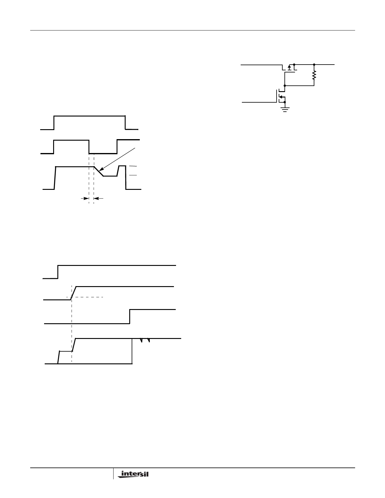
Low to high transition is determined primarily by the switch
resistance and the external capacitive load. High to low
transition is more complex. Take the case where the block is
already enabled (VDPM is H). When VFLK is H, pin CE is
grounded. On the falling edge of VFLK, a current is passed
into pin CE, to charge an external capacitor to 1.2V. This
creates a delay, equal to CE * 4200. At this point, the output
begins to pull down from VGH to VDD1. The slew current is
equal to 300/(RE+5000)*Load Capacitance.
the following circuit can be inserted between input and
inductor to disconnect the DC path when the part is disabled.
TO INDUCTOR
INPUT
ENABLE
VDPM
0
VFLK
0
VGH_M
0
SLOPE CONTROLLED
BY RE AND LOAD
CAPACITANCE
VGH
VDD_1
DELAY TIME
CONTROLLED BY CE
FIGURE 15. GATE PULSE MODULATOR TIMING DIAGRAM
Start-Up Sequence
Figure 16 shows a detailed start-up sequence waveform.
VIN
0
ENABLE
0
VDPM
0
VIN THRESHOLD
AVDD
VGH_M
0
FIGURE 16. START-UP SEQUENCE
FIGURE 17. CIRCUIT TO DISCONNECT THE DC PATH OF
BOOST CONVERTER
VCOM Amplifier
The VCOM amplifier is designed to control the voltage on the
back plate of an LCD display. This plate is capacitively
coupled to the pixel drive voltage which alternately cycles
positive and negative at the line rate for the display. Thus the
amplifier must be capable of sourcing and sinking capacitive
pulses of current, which can occasionally be quite large (a
few 100mA for typical applications).
The ISL97645 VCOM amplifier's output current is limited to
400mA. This limit level, which is roughly the same for
sourcing and sinking, is included to maintain reliable
operation of the part. It does not necessarily prevent a large
temperature rise if the current is maintained. (In this case the
whole chip may be shut down by the thermal trip to protect
functionality.) If the display occasionally demands current
pulses higher than this limit, the reservoir capacitor will
provide the excess and the amplifier will top the reservoir
capacitor back up once the pulse has stopped. This will
happen on the µs time scale in practical systems and for
pulses 2 or 3 times the current limit, the VCOM voltage will
have settled again before the next line is processed.
Fault Protection
ISL97645 provides the overall fault protections including
over current protection and over-temperature protection.
An internal temperature sensor continuously monitors the
die temperature. In the event that die temperature exceeds
the thermal trip point, the device will shut down and disable
itself. The upper and lower trip points are typically set to
140°C and 100°C respectively.
When VIN exceeds 2.5V and ENABLE reaches the VIH
threshold value, Boost converter starts up, and gate pulse
modulator circuit output holds until VDPM goes to high. Note
that there is a DC path in the boost converter from the input
to the output through the inductor and diode, hence the input
voltage will be seen at output with a forward voltage drop of
diode before the part is enabled. If this voltage is not desired,
12
FN9263.0
April 11, 2006
Share Link: 