IDT74SSTUBF32869A 데이터 시트보기 (PDF) - Integrated Device Technology
부품명
상세내역
일치하는 목록
IDT74SSTUBF32869A Datasheet PDF : 22 Pages
| |||
IDT74SSTUBF32869A
14-BIT CONFIGURABLE REGISTERED BUFFER FOR DDR2
COMMERCIAL TEMPERATURE GRADE
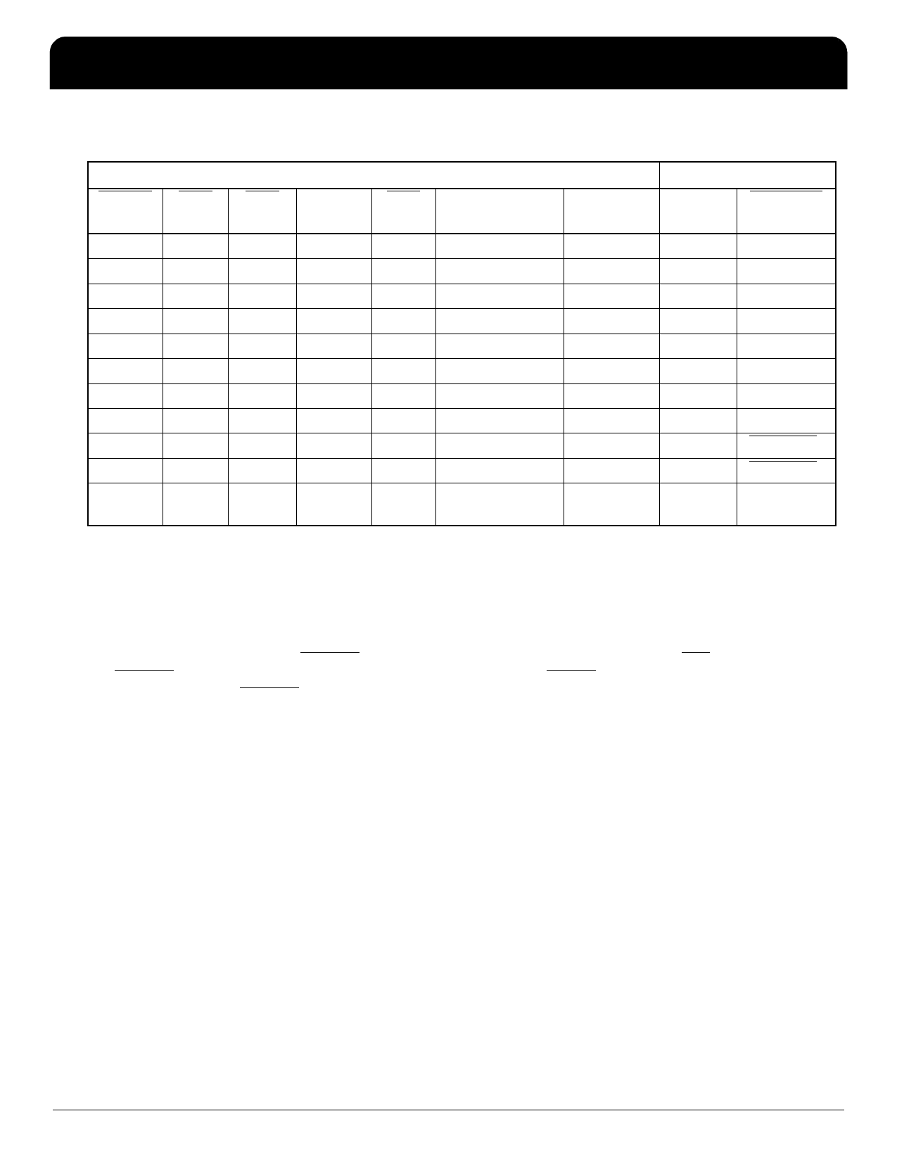
Parity and Standby Function Table
RESET DCS CSR
Inputs1
CLK CLK
Σ of Inputs = H
(D1 - D14)2
PARIN3
Outputs
PPO PTYERR4
H
L
X
↑
↓
Even
L
L
H
H
L
X
↑
↓
Odd
L
H
L
H
L
X
↑
↓
Even
H
H
L
H
L
X
↑
↓
Odd
H
L
H
H
L
L
↑
↓
Even
L
L
H
H
L
L
↑
↓
Odd
L
H
L
H
L
L
↑
↓
Even
H
H
L
H
L
L
↑
↓
Odd
H
L
H
H
H
H
↑
↓
X
X
PPOn0 PTYERRn0
H
X
X
L or H L or H
X
X
PPOn0 PTYERRn0
L
X or
X or
X or
X or
X or Floating X or Floating
L
H
Floating Floating Floating Floating
1 H = HIGH Voltage Level
L = LOW Voltage Level
X = Don’t Care
↑ = LOW to HIGH
↓ = HIGH to LOW
2 This range does not include D1, D4, and D7.
3 PARIN arrives one clock cycle (C1 = 0), or two clock cycles (C1 = 1), after the data to which it applies.
4 This transition assumes PTYERR is HIGH at the crossing of CLK going HIGH and CLK going LOW. If
PTYERR is LOW, it stays latched LOW for two clock cycles or until RESET is driven LOW. PARIN is used to
generate PPO and PTYERR.
14-BIT CONFIGURABLE REGISTERED BUFFER FOR DDR2
8
CONFIDENTIAL
IDT74SSTUBF32869A
7093/8
Share Link: 