IDT74FCT827AL 데이터 시트보기 (PDF) - Integrated Device Technology
부품명
상세내역
일치하는 목록
IDT74FCT827AL Datasheet PDF : 7 Pages
| |||
IDT54/74FCT827A/B/C
HIGH-PERFORMANCE CMOS BUFFERS
MILITARY AND COMMERCIAL TEMPERATURE RANGES
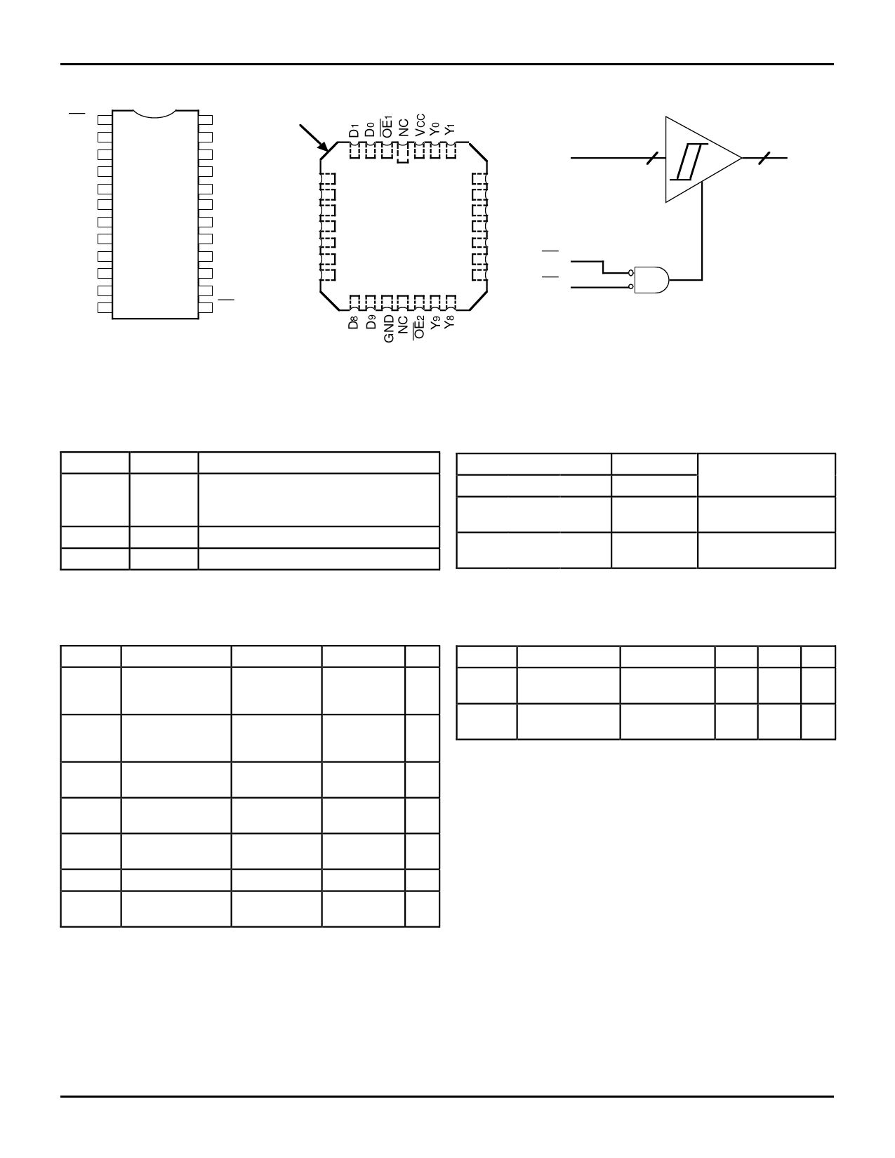
PIN CONFIGURATIONS
OE1 1
24 VCC INDEX
D0 2
23 Y0
D1 3
22 Y1
D2 4 P24-1 21 Y2
D3 5 D24-1 20 Y3
D4 6 E24-1 19 Y4
D5 7 & 18 Y5
D6 8 SO24-2 17 Y6
D7 9
16 Y7
D8 10
15 Y8
D9 11
GND 12
14 Y9
13 OE2
D2
4
5
3
2
1
28 27 26
25
Y2
D3 6
24 Y3
D4 7
23 Y4
NC 8
D5 9
L28-1
22 NC
21 Y5
D6 10
20 Y6
D7 11
19 Y7
1213 14 15 16 17 18
LOGIC SYMBOL
10
D0-9
OE1
OE2
10
Y0-9
2609 drw 04
2609 drw 02
DIP/CERPACK/SOIC
TOP VIEW
LCC
TOP VIEW
2609 drw 03
PIN DESCRIPTION
Name
OEI
DI
YI
I/O
Description
I
When both are LOW, the outputs are
enabled. When either one or both are
HIGH, the outputs are High Z.
I
10-bit data input.
O 10-bit data output.
2609 tbl 02
FUNCTION TABLE(1)
Inputs
Output
OE1 OE2
DI
YI
Function
L
L
L
L
L
L
H
H
H
X
X
Z
X
H
X
Z
Transparent
Three-State
NOTE:
1. H = HIGH, L = LOW, X = Don’t Care, Z = High Impedance
2609 tbl 03
ABSOLUTE MAXIMUM RATINGS(1)
Symbol
Rating
VTERM(2) Terminal Voltage
with Respect to
GND
VTERM(3) Terminal Voltage
with Respect to
GND
TA
Operating
Temperature
TBIAS Temperature
Under Bias
TSTG Storage
Temperature
Commercial
–0.5 to +7.0
–0.5 to VCC
0 to +70
–55 to +125
–55 to +125
Military Unit
–0.5 to +7.0 V
–0.5 to VCC V
–55 to +125 °C
–65 to +135 °C
–65 to +150 °C
PT
Power Dissipation
0.5
0.5
W
IOUT
DC Output
120
120
mA
Current
NOTES:
2609 tbl 04
1. Stresses greater than those listed under ABSOLUTE MAXIMUM
RATINGS may cause permanent damage to the device. This is a stress
rating only and functional operation of the device at these or any other
conditions above those indicated in the operational sections of this
specification is not implied. Exposure to absolute maximum rating con-
ditions for extended periods may affect reliability. No terminal voltage may
exceed VCC by +0.5V unless otherwise noted.
2. Input and VCC terminals only.
3. Outputs and I/O terminals only.
CAPACITANCE (TA = +25°C, f = 1.0MHz)
Symbol Parameter(1)
CIN
Input
Capacitance
COUT Output
Capacitance
Conditions Typ. Max. Unit
VIN = 0V
6 10 pF
VOUT = 0V
8 12 pF
NOTE:
2609 tbl 05
1. This parameter is measured at characterization but not tested.
7.20
2
Share Link: 