IDT7132 데이터 시트보기 (PDF) - Integrated Device Technology
부품명
상세내역
일치하는 목록
IDT7132 Datasheet PDF : 16 Pages
| |||
IDT7132SA/LA and IDT 7142SA/LA
High Speed 2K x 8 Dual Port Static RAM
Military, Industrial and Commercial Temperature Ranges
Description
The IDT7132/IDT7142 are high-speed 2K x 8 Dual-Port Static RAMs.
The IDT7132 is designed to be used as a stand-alone 8-bit Dual-Port RAM
or as a “MASTER” Dual-Port RAM together with the IDT7142 “SLAVE”
Dual-Port in 16-bit-or-more word width systems. Using the IDT MASTER/
SLAVE Dual-Port RAM approach in 16-or-more-bit memory system
applications results in full-speed, error-free operation without the need for
additional discrete logic.
Both devices provide two independent ports with separate control,
address, and l/O pins that permit independent, asynchronous access for
reads or writes to any location in memory. An automatic power down
feature, controlled by CE permits the on-chip circuitry of each port to enter
a very low standby power mode.
Fabricated using IDT’s CMOS high-performance technology, these
devices typically operate on only 325mW of power. Low-power (LA)
versions offer battery backup data retention capability, with each Dual-
Port typically consuming 200µW from a 2V battery.
The IDT7132/7142 devices are packaged in a 48-pin sidebraze or
plastic DIPs, 48-pin LCCs, 52-pin PLCCs, and 48-lead flatpacks.
Military grade product is manufactured in compliance with the latest
revision of MIL-PRF-38535 QML, making it ideally suited to military
temperature applications demanding the highest level of performance
and reliability.
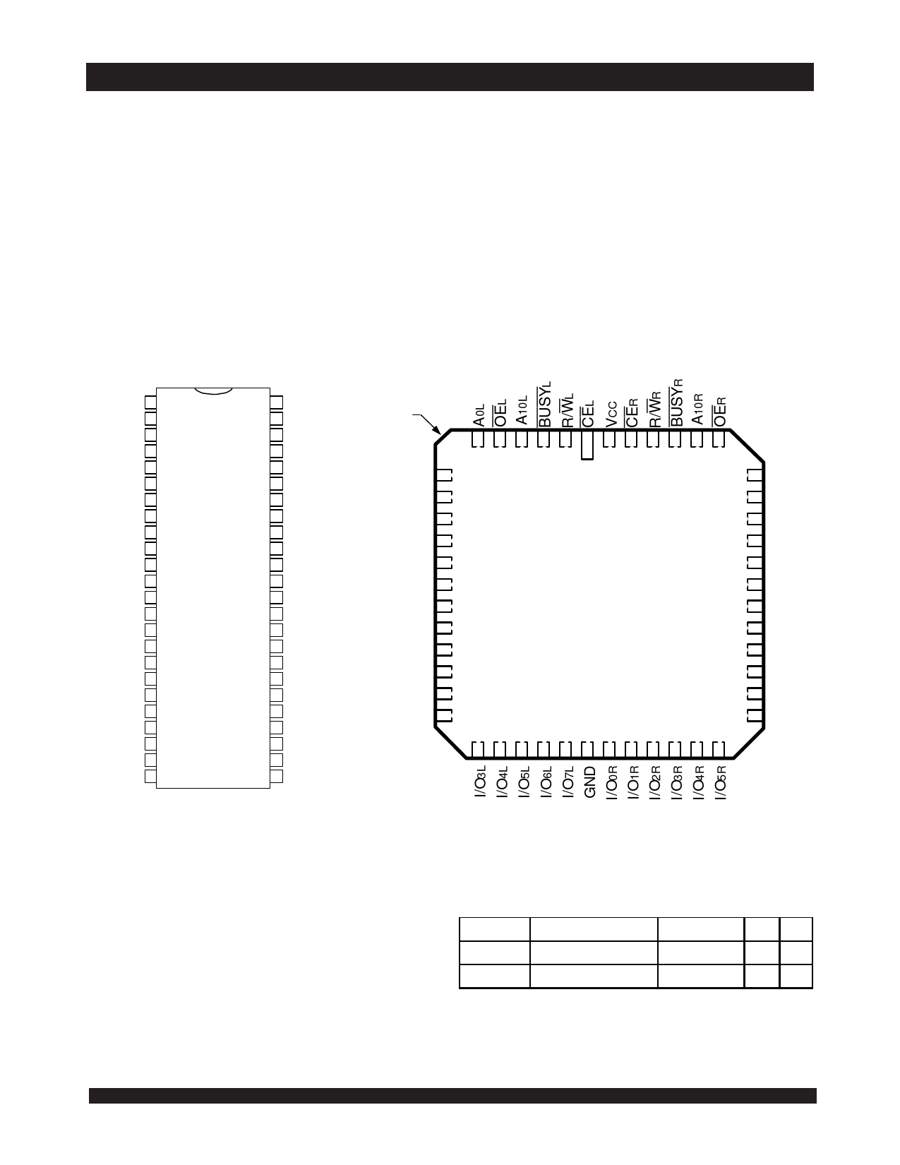
Pin Configurations(1,2,3)
CEL
R/WL
BUSYL
A10L
OEL
A0L
A1L
A2L
A3L
A4L
A5L
A6L
A7L
A8L
A9L
I/O0L
I/O1L
I/O2L
I/O3L
I/O4L
I/O5L
I/O6L
I/O7L
GND
1
48
2
47
3
46
4
45
5
44
6
7
8
9
IDT7132/
7142
P or C
43
42
41
40
10
39
11
12
P48-1(4)
&
38
37
13
14
C48-2(4)
36
35
15 48-Pin 34
16 DIP 33
17 Top 32
18 View(5) 31
19
30
20
29
21
28
22
27
23
26
24
25
VCC
CER
R/WR
INDEX
BUSYR
A10R
OER
A1L
A0R
A2L
A1R
A3L
A2R
A3R
A4L
A4R
A5L
A5R
A6L
A6R
A7R
A7L
A8R
A8L
A9R
I/O7R
I/O6R
A9L
I/O0L
I/O5R
I/O1L
I/O4R
I/O3R
I/O2L
I/O2R
I/O1R
I/O0R
,
2692 drw 02
NOTES:
1. All VCC pins must be connected to the power supply.
2. All GND pins must be connected to the ground supply.
3. P48-1 package body is approximately .55 in x 2.43 in x .18 in.
C48-2 package body is approximately .62 in x 2.43 in x .15 in.
L48-1 package body is approximately .57 in x .57 in x .68 in.
F48-1 package body is approximately .75 in x .75 in x .11 in.
4. This package code is used to reference the package diagram.
5. This text does not indicate orientation of the actual part-marking.
6 5 4 3 2 48 47 46 45 44 43
7
1
42 A0R
8
41 A1R
9
40 A2R
10
IDT7132/42L48 or F
39 A3R
11
L48-1(4)
38 A4R
12
&
F48-1(4)
37 A5R
13
36 A6R
48-Pin LCC/ Flatpack
14
Top View(5)
35 A7R
15
34 A8R
16
33 A9R
17
32 I/O7R
18
31 I/O6R
19 20 21 22 23 24 25 26 27 28 29 30
,
2692 drw 03
Capacitance(1) (TA = +25°C,f = 1.0MHz)
Symbol
Parameter
Conditions(2) Max. Unit
CIN
Input Capacitance
VIN = 3dV
11 pF
COUT Output Capacitance
VOUT = 3dV
11 pF
NOTES:
2692 tbl 00
1. This parameter is determined by device characterization but is not production
tested.
2. 3dV represents the interpolated capacitance when the input and output signals
switch from 3V to 0V.
2
Share Link: 