IDT2305A 데이터 시트보기 (PDF) - Integrated Device Technology
부품명
상세내역
일치하는 목록
IDT2305A Datasheet PDF : 7 Pages
| |||
IDT2305A
3.3V ZERO DELAY CLOCK BUFFER
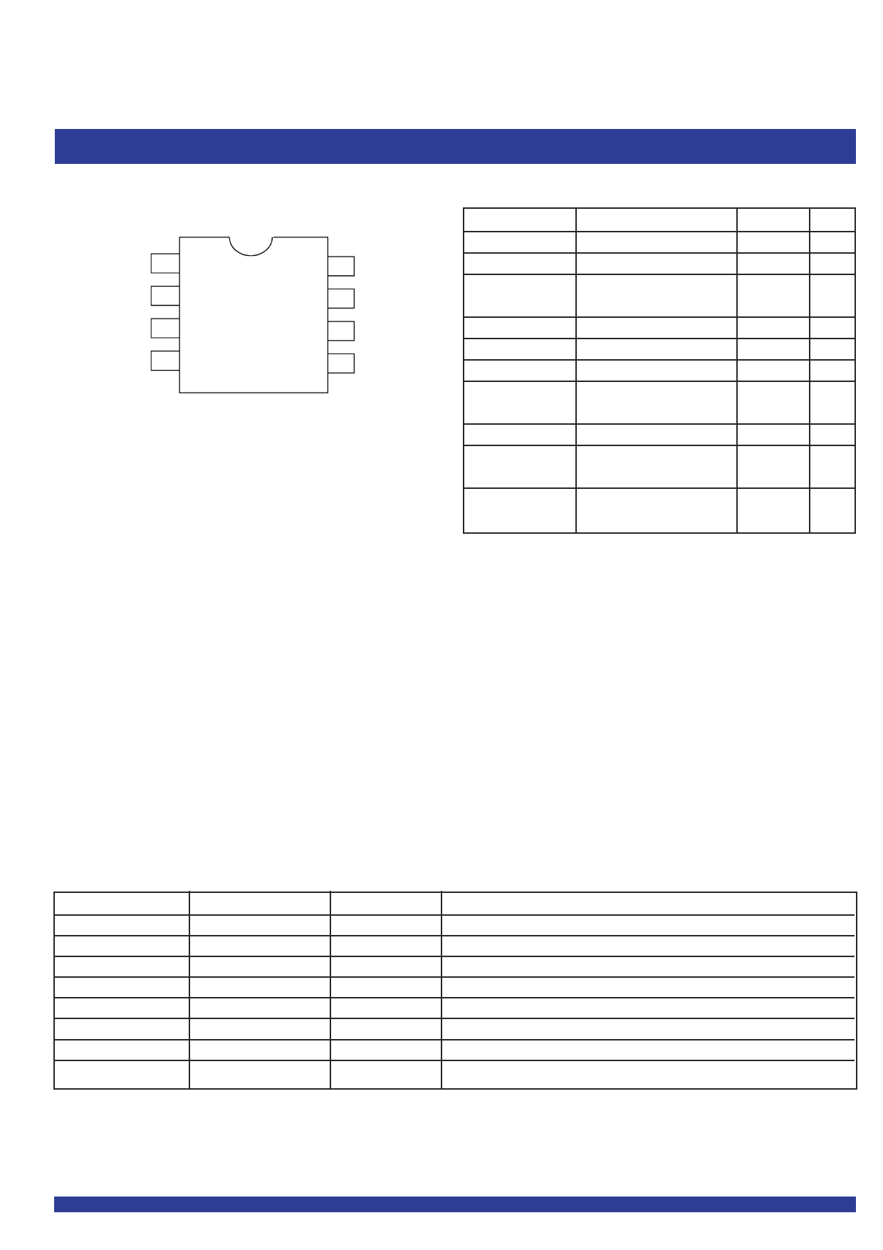
PIN CONFIGURATION
REF
1
8
CLK2
2
7
CLK1
3
6
GND
4
5
SOIC
TOP VIEW
APPLICATIONS:
• SDRAM
• Telecom
• Datacom
• PC Motherboards/Workstations
• Critical Path Delay Designs
CLKOUT
CLK4
VDD
CLK3
COMMERCIAL AND INDUSTRIAL TEMPERATURE RANGES
ABSOLUTE MAXIMUM RATINGS(1)
Symbol
VDD
VI (2)
VI
IIK (VI < 0)
IO (VO = 0 to VDD)
VDD or GND
TA = 55°C
(in still air)(3)
TSTG
Operating
Temperature
Operating
Temperature
Rating
Supply Voltage Range
Input Voltage Range (REF)
Input Voltage Range
(except REF)
Input Clamp Current
Continuous Output Current
Continuous Current
Maximum Power Dissipation
Max.
Unit
–0.5 to +4.6 V
–0.5 to +5.5 V
–0.5 to
V
VDD+0.5
–50
mA
±50
mA
±100
mA
0.7
W
Storage Temperature Range
Commercial Temperature
Range
Industrial Temperature
Range
–65 to +150 °C
0 to +70 °C
-40 to +85 °C
NOTES:
1. Stresses greater than those listed under ABSOLUTE MAXIMUM RATINGS may cause
permanent damage to the device. This is a stress rating only and functional operation
of the device at these or any other conditions above those indicated in the operational
sections of this specification is not implied. Exposure to absolute maximum rating
conditions for extended periods may affect reliability.
2. The input and output negative-voltage ratings may be exceeded if the input and output
clamp-current ratings are observed.
3. The maximum package power dissipation is calculated using a junction temperature
of 150°C and a board trace length of 750 mils.
PIN DESCRIPTION
Pin Name
REF(1)
CLK2(2)
CLK1(2)
GND
CLK3(2)
VDD
CLK4(2)
CLKOUT(2)
Pin Number
1
2
3
4
5
6
7
8
NOTES:
1. Weak pull down.
2. Weak pull down on all outputs.
Type
IN
Out
Out
Ground
Out
PWR
Out
Out
Functional Description
Input reference clock, 5 Volt tolerant input
Output clock
Output clock
Ground
Output clock
3.3V Supply
Output clock
Output clock, internal feedback on this pin
2
Share Link: 