80C86 데이터 시트보기 (PDF) - Intersil
부품명
상세내역
일치하는 목록
80C86 Datasheet PDF : 37 Pages
| |||
80C86
edge of this pulse, a valid address and certain status
information for the cycle may be latched.
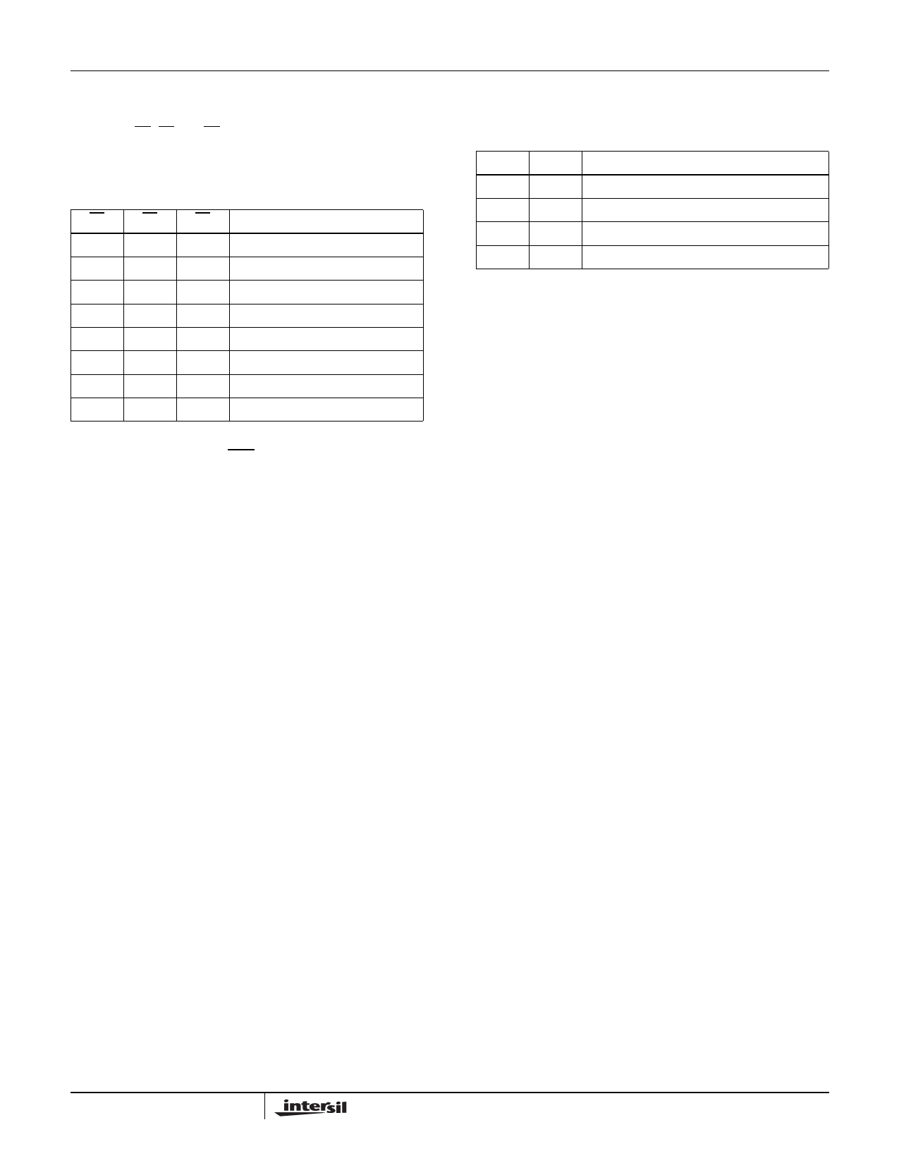
Status bits S0, S1 and S2 are used by the bus controller, in
maximum mode, to identify the type of bus transaction
according to Table 2.
TABLE 2.
S2
S1
S0
CHARACTERISTICS
0
0
0 Interrupt
0
0
1 Read I/O
0
1
0 Write I/O
0
1
1 Halt
1
0
0 Instruction Fetch
1
0
1 Read Data from Memory
1
1
0 Write Data to Memory
1
1
1 Passive (No Bus Cycle)
Status bits S3 through S7 are time multiplexed with high
order address bits and the BHE signal, and are therefore
valid during t2 through t4. S3 and S4 indicate which segment
register (see “Instruction Set Summary” on page 31) was
used for this bus cycle in forming the address, according to
Table 3.
S5 is a reflection of the PSW interrupt enable bit. S3 is
always zero and S7 is a spare status bit.
TABLE 3.
S4
S3
CHARACTERISTICS
0
0 Alternate Data (Extra Segment)
0
1 Stack
1
0 Code or None
1
1 Data
I/O Addressing
In the 80C86, I/O operations can address up to a maximum
of 64k I/O byte registers or 32k I/O word registers. The I/O
address appears in the same format as the memory address
on bus lines A15-A0. The address lines A19-A16 are zero in
I/O operations. The variable I/O instructions which use
register DX as a pointer have full address capability while
the direct I/O instructions directly address one or two of the
256 I/O byte locations in page 0 of the I/O address space.
I/O ports are addressed in the same manner as memory
locations. Even addressed bytes are transferred on the D7-D0
bus lines and odd addressed bytes on D15-D8. Care must be
taken to ensure that each register within an 8-bit peripheral
located on the lower portion of the bus be addressed as even.
10
FN2957.3
January 9, 2009
Share Link: 