ICS9248-195 데이터 시트보기 (PDF) - Integrated Circuit Systems
부품명
상세내역
일치하는 목록
ICS9248-195
Integrated Circuit Systems

ICS9248-195 Datasheet PDF : 16 Pages
| |||
ICS9248 - 195
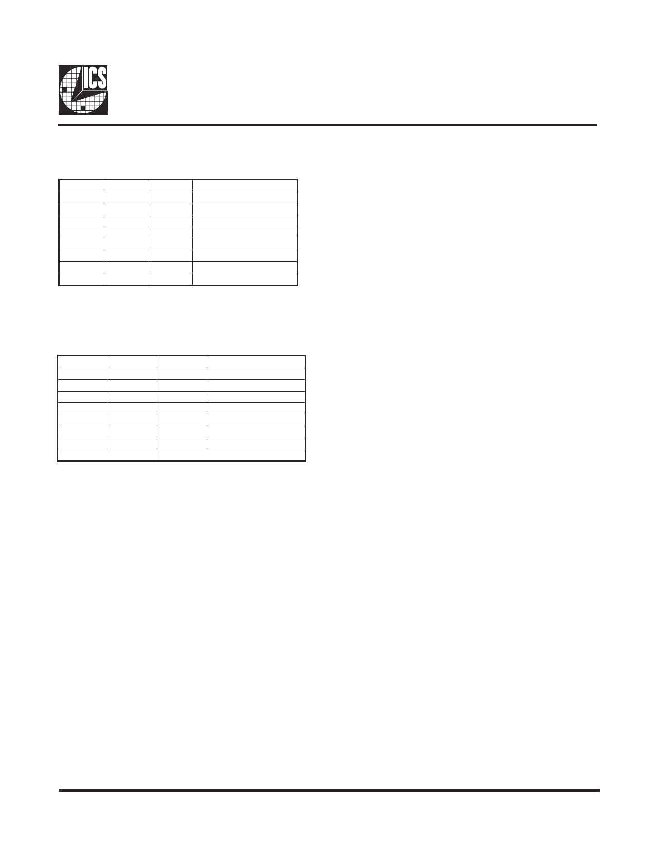
Byte 4: Active/Inactive Register (1 = enable, 0 = disable)
Bit
Bit 7
Bit 6
Bit 5
Bit 4
Bit 3
Bit 2
Bit 1
Bit 0
Pin #
-
-
-
-
-
-
-
-
PWD
1
0
0
0
0
0
0
1
Description
(Reserved)
(Reserved)
(SEL24_48)#
Latched FS0#
Latched FS1#
Latched FS2#
Latched FS3#
(Reserved)
Byte 5: Active/Inactive Register (1 = enable, 0 = disable)
Bit
Bit 7
Bit 6
Bit 5
Bit 4
Bit 3
Bit 2
Bit 1
Bit 0
Pin #
34
35
37
38
26
25
48
2
PWD
1
1
1
1
1
1
1
1
Description
SDRAM3 (En/Dis)
SDRAM2 (En/Dis)
SDRAM1 (En/Dis)
SDRAM0 (En/Dis)
48MHz (En/Dis)
24MHz (En/Dis)
REF1 (En/Dis)
REF0 (En/Dis)
Notes:
1. Inactive means outputs are held LOW and are disabled from switching.
2. Latched register values will be inverted from pin values. Default latch condition is for all latched inputs to be floating
(pulled up via internal resistor) at power-up.
0375D—02/02/04
5
Share Link: