AV9148F-53 데이터 시트보기 (PDF) - Integrated Circuit Systems
부품명
상세내역
일치하는 목록
AV9148F-53 Datasheet PDF : 18 Pages
| |||
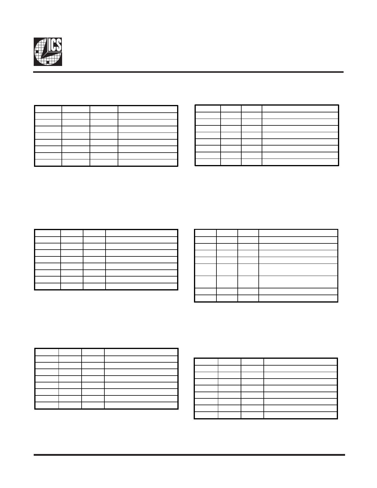
ICS9148 - 53
Byte 1: CPU, Active/Inactive Register
(1 = enable, 0 = disable)
B it
Bit 7
Bit 6
Bit 5
Bit 4
Bit 3
Bit 2
Bit 1
Bit 0
Pin #
-
-
-
40
-
41
43
44
PWD
1
1
1
1
1
1
1
1
D e s cription
(R e se rve d )
(R e se rve d )
(R e se rve d )
SDRAM 12 (Act/Inact)
(R e se rve d )
C P UC LK 2 (Act/Inact)
C P UC LK 1 (Act/Inact)
C P UC LK 0 (Act/Inact)
Notes:
1. Inactive means outputs are held LOW and are disabled
from switching.
Byte 2: PCI Active/Inactive Register
(1 = enable, 0 = disable)
B it
Bit 7
Bit 6
Bit 5
Bit 4
Bit 3
Bit 2
Bit 1
Bit 0
Pin #
-
7
-
13
12
11
10
8
PWD
1
1
1
1
1
1
1
1
D e s cription
(R e se rve d )
P C IC LK _F (Act/Inact)
(R e se rve d )
P C IC LK 4 (Act/Inact)
P C IC LK 3 (Act/Inact)
P C IC LK 2 (Act/Inact)
P C IC LK 1 (Act/Inact)
P C IC LK 0(Act/Inact)
Notes:
1. Inactive means outputs are held LOW and are disabled
from switching.
Byte 3: SDRAM Active/Inactive Register
(1 = enable, 0 = disable)
Bit
Bit 7
Bit 6
Bit 5
Bit 4
Bit 3
Bit 2
Bit 1
Bit 0
Pin #
28
29
31
32
34
35
37
38
PWD
1
1
1
1
1
1
1
1
Description
SDRAM7 (Act/Inact)
SDRAM6 (Act/Inact)
SDRAM5 (Act/Inact)
SDRAM4 (Act/Inact)
SDRAM3 (Act/Inact)
SDRAM2 (Act/Inact)
SDRAM1 (Act/Inact)
SDRAM0 (Act/Inact)
Notes:
1. Inactive means outputs are held LOW and are disabled
from switching.
Byte 5: Peripheral Active/Inactive Register
(1 = enable, 0 = disable)
Bit
Bit 7
Bit 6
Bit 5
Bit 4
Bit 3
Bit 2
Bit 1
Bit 0
Pin #
-
8
7
47
-
2
46
2
PWD
1
-
-
1
1
-
1
1
Description
(Reserved)
FS2#
FS1#
PCICLK5 (Act/Inact)
(Reserved)
FS3#
AGP1 (Act/Inact)
REF0 (Act/Inact)
Notes:
1. Inactive means outputs are held LOW and are disabled
from switching.
Byte 4: SDRAM Active/Inactive Register
(1 = enable, 0 = disable)
B it
Bit 7
Bit 6
Bit 5
Bit 4
Bit 3
Bit 2
Bit 1
Bit 0
Pin #
25
-
26
-
17
18
20
21
PWD
1
1
-
1
1
1
1
1
D e s cription
AGP0 (Active/Inactive)
(R e se rve d )
FS0#
(R e se rve d )
SDRAM 11 (Act/Inact)
(Desktop M ode O nly)
SDRAM 10 (Act/Inact)
(Desktop M ode O nly)
SDRAM 9 (Act/Inact)
SDRAM 8 (Act/Inact)
Notes:
1. Inactive means outputs are held LOW and are disabled
from switching.
Byte 6: Optional Register for Possible
Furture Requirements
Bit
Bit 7
Bit 6
Bit 5
Bit 4
Bit 3
Bit 2
Bit 1
Bit 0
Pin #
-
-
-
-
-
-
-
-
PWD
1
1
1
1
1
1
1
1
Description
(Reserved)
(Reserved)
(Reserved)
(Reserved)
(Reserved)
(Reserved)
(Reserved)
(Reserved)
Notes:
1. Byte 6 is reserved by Integrated Circuit Systems for futue
applications.
7
Share Link: 