HY57V641620ELT 데이터 시트보기 (PDF) - Hynix Semiconductor
부품명
상세내역
일치하는 목록
HY57V641620ELT Datasheet PDF : 13 Pages
| |||
Synchronous DRAM Memory 64Mbit (4Mx16bit)
HY57V641620E(L/S)T(P) Series
DESCRIPTION
The Hynix HY57V641620E(L/S)T(P) series is a 67,108,864bit CMOS Synchronous DRAM, ideally suited for the memory
applications which require wide data I/O and high bandwidth. HY57V641620E(L/S)T(P) is organized as 4banks of
1,048,576x16.
HY57V641620E(L/S)T(P) is offering fully synchronous operation referenced to a positive edge of the clock. All inputs
and outputs are synchronized with the rising edge of the clock input. The data paths are internally pipelined to achieve
very high bandwidth. All input and output voltage levels are compatible with LVTTL.
Programmable options include the length of pipeline (Read latency of 2 or 3), the number of consecutive read or write
cycles initiated by a single control command (Burst length of 1,2,4,8 or full page), and the burst count sequence(se-
quential or interleave). A burst of read or write cycles in progress can be terminated by a burst terminate command or
can be interrupted and replaced by a new burst read or write command on any cycle. (This pipelined design is not re-
stricted by a '2N' rule)
FEATURES
• Voltage: VDD, VDDQ 3.3V supply voltage
• Auto refresh and self refresh
• All device pins are compatible with LVTTL interface • 4096 Refresh cycles / 64ms
• 54 Pin TSOPII (Lead or Lead Free Package)
• Programmable Burst Length and Burst Type
• All inputs and outputs referenced to positive edge of
system clock
• Data mask function by UDQM, LDQM
• Internal four banks operation
- 1, 2, 4, 8 or full page for Sequential Burst
- 1, 2, 4 or 8 for Interleave Burst
• Programmable CAS Latency; 2, 3 Clocks
• Burst Read Single Write operation
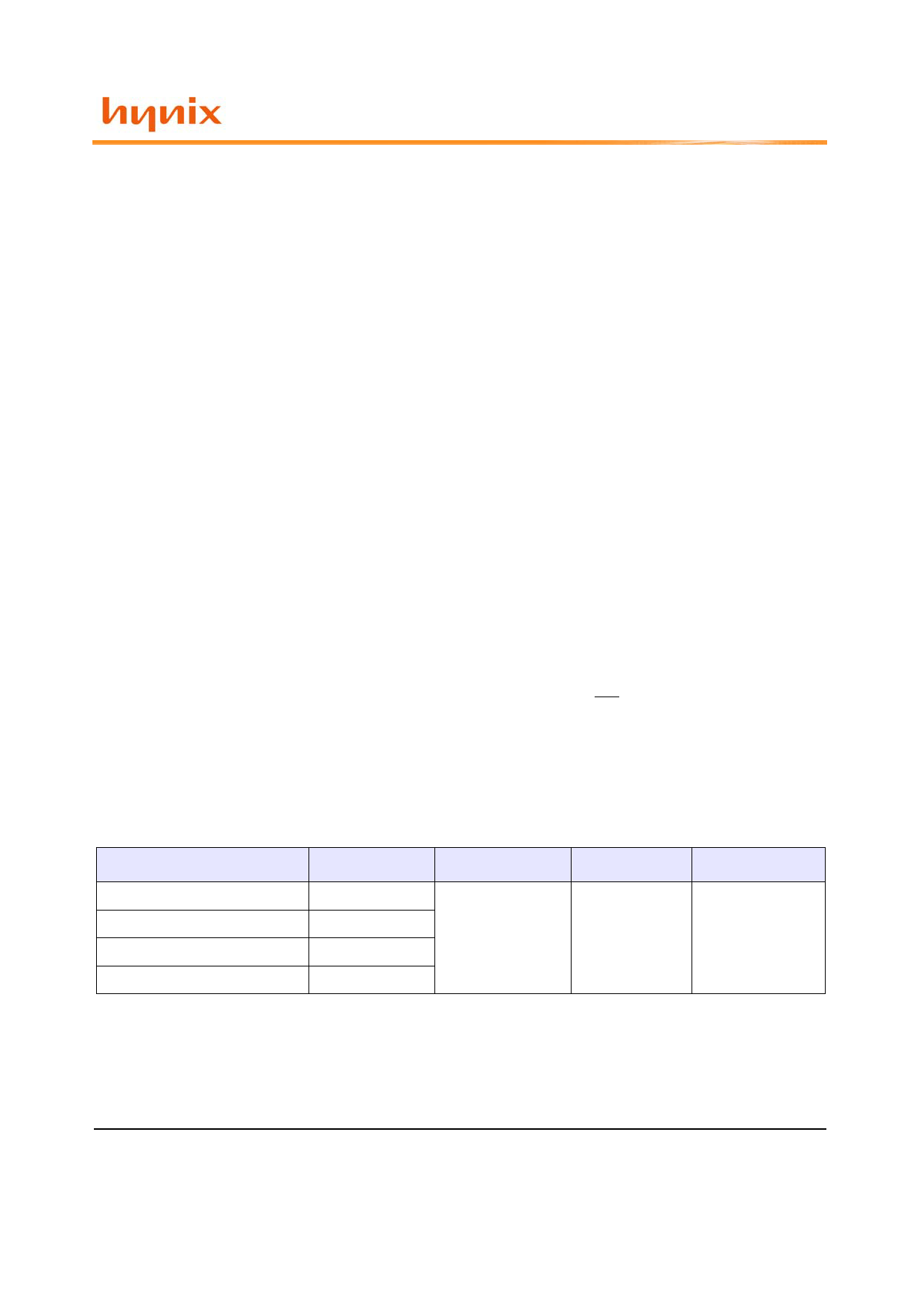
ORDERING INFORMATION
Part No.
HY57V641620E(L/S)T(P)-5
HY57V641620E(L/S)T(P)-6
HY57V641620E(L/S)T(P)-7
HY57V641620E(L/S)T(P)-H
Clock Frequency
Organization
200MHz
166MHz
143MHz
133MHz
4Banks x 1Mbits x16
Note: 1. HY57V641620ET Series: Normal power, Leaded.
2. HY57V641620ELT Series: Low power, Leaded.
3. HY57V641620EST Series: Super Low power, Leaded.
4. HY57V641620ETP Series: Normal power, Lead Free.
5. HY57V641620ELTP Series: Low power, Lead Free.
6. HY57V641620ESTP Series: Super Low Power, Lead Free
Rev. 1.5 / Feb. 2005
Interface
LVTTL
Package
54 Pin TSOPII
2
Share Link: 