HSP3824 데이터 시트보기 (PDF) - Harris Semiconductor
부품명
상세내역
일치하는 목록
HSP3824 Datasheet PDF : 41 Pages
| |||
HSP3824
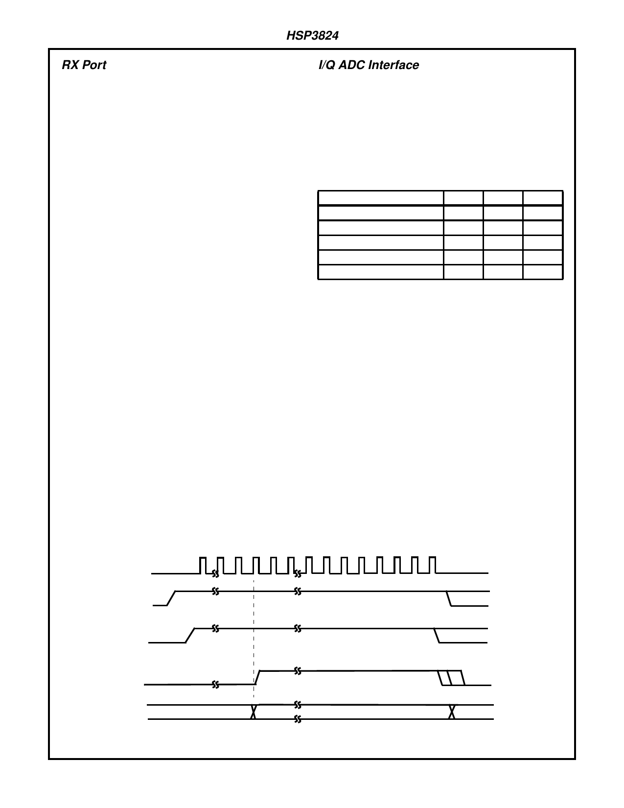
RX Port
I/Q ADC Interface
The timing diagram Figure 7 illustrates the relationships
between the various signals of the RX port. The receive data
port serially outputs the demodulated data from RXD. The
data is output as soon as it is demodulated by the HSP3824.
RX_PE must be at its active state throughout the receive
operation. When RX_PE is inactive the device's receive
functions, including acquisition, will be in a stand by mode.
RXCLK is an output from the HSP3824 and is the clock for
the serial demodulated data on RXD. MD_RDY is an output
from the HSP3824 and it envelopes the valid data on RXD.
The HSP3824 can be also programmed to ignore error
detections during the CCITT - CRC 16 check of the header
fields. If programmed to ignore errors the device continues to
output the demodulated data in its entirety regardless of the
CCITT - CRC 16 check result. This option is programmed
through CR 2, bit 5.
Note that RXCLK becomes active after acquisition, well
before valid data begins to appear on RXD and MD_RDY is
asserted. MD_RDY returns to its inactive state under the fol-
lowing conditions:
• The number of data symbols, as defined by the length field
in the protocol, has been received and output through
RXD in its entirety (normal condition).
• PN tracking is lost during demodulation.
• RX_PE is deactivated by the external controller.
MD_RDY can be configured through CR 9, bit 6 to be active
low, or active high. Energy Detect (ED) pin 45 (Test port),
and Carrier Sense (CRS) pin 46 (Test port), are available
outputs from the HSP3824 and can be useful signals for an
effective RX interface design. Use of these signals is
optional. CRS and ED are further described within this docu-
ment. The receive port is completely independent from the
operation of the other interface ports including the TX port,
supporting therefore a full duplex mode.
The PRISM baseband processor chip (HSP3824) includes
two 3-bit Analog to Digital converters (ADCs) that sample
the analog input from the IF down converter. The I/Q ADC
clock, MCLK, samples at twice the chip rate. The maximum
sampling rate is 44MHz (power supply: 3.3V to 5.0V) or
33MHz (power supply 2.7V to 5.5V).
The interface specifications for the I and Q ADCs are listed
on Table 2 below.
TABLE 2. I, Q, ADC SPECIFICATIONS
PARAMETER
MIN
TYP
MAX
Full Scale Input Voltage (VP-P)
Input Bandwidth (-0.5dB)
0.25
0.50
1.0
-
20MHz
-
Input Capacitance (pF)
-
5
-
Input Impedance (DC)
5kΩ
-
-
FS (Sampling Frequency)
-
-
44MHz
The voltages applied to pin 16,VREFP and pin 17, VREFN set
the references for the internal I and Q ADC converters. In
addition, VREFP is also used to set the RSSI ADC converter
reference. For a nominal 500mVP-P, the suggested VREFP
voltage is 1.75V, and the suggested VREFN is 0.93V. VREFN
should never be less than 0.25V. Since these ADCs are
intended to sample AC voltages, their inputs are biased
internally and they should be capacitively coupled.
The ADC section includes a compensation (calibration) cir-
cuit that automatically adjusts for temperature and compo-
nent variations of the RF and IF strips. The variations in gain
of limiters, AGC circuits, filters etc. can be compensated for
up to ±4dB. Without the compensation circuit, the ADCs
could see a loss of up to 1.5 bits of the 3 bits of quantization.
The ADC calibration circuit adjusts the ADC reference volt-
ages to maintain optimum quantization of the IF input over
this variation range. It works on the principle of setting the
reference to insure that the signal is at full scale (saturation)
a certain percentage of the time. Note that this is not an
AGC and it will compensate only for slow variations in signal
levels (several seconds).
RXCLK
RX_PE
CRS (TEST 7)
MD_RDY
PROCESSING
PREAMBLE/HEADER
RXD
NOTE: MD_RDY active after CRC16.
LSB
DATA
FIGURE 7. RX PORT TIMING
11
MSB
Share Link: 