LT1251 데이터 시트보기 (PDF) - Linear Technology
부품명
상세내역
일치하는 목록
LT1251 Datasheet PDF : 24 Pages
| |||
LT1251/LT1256
APPLICATIONS INFORMATION
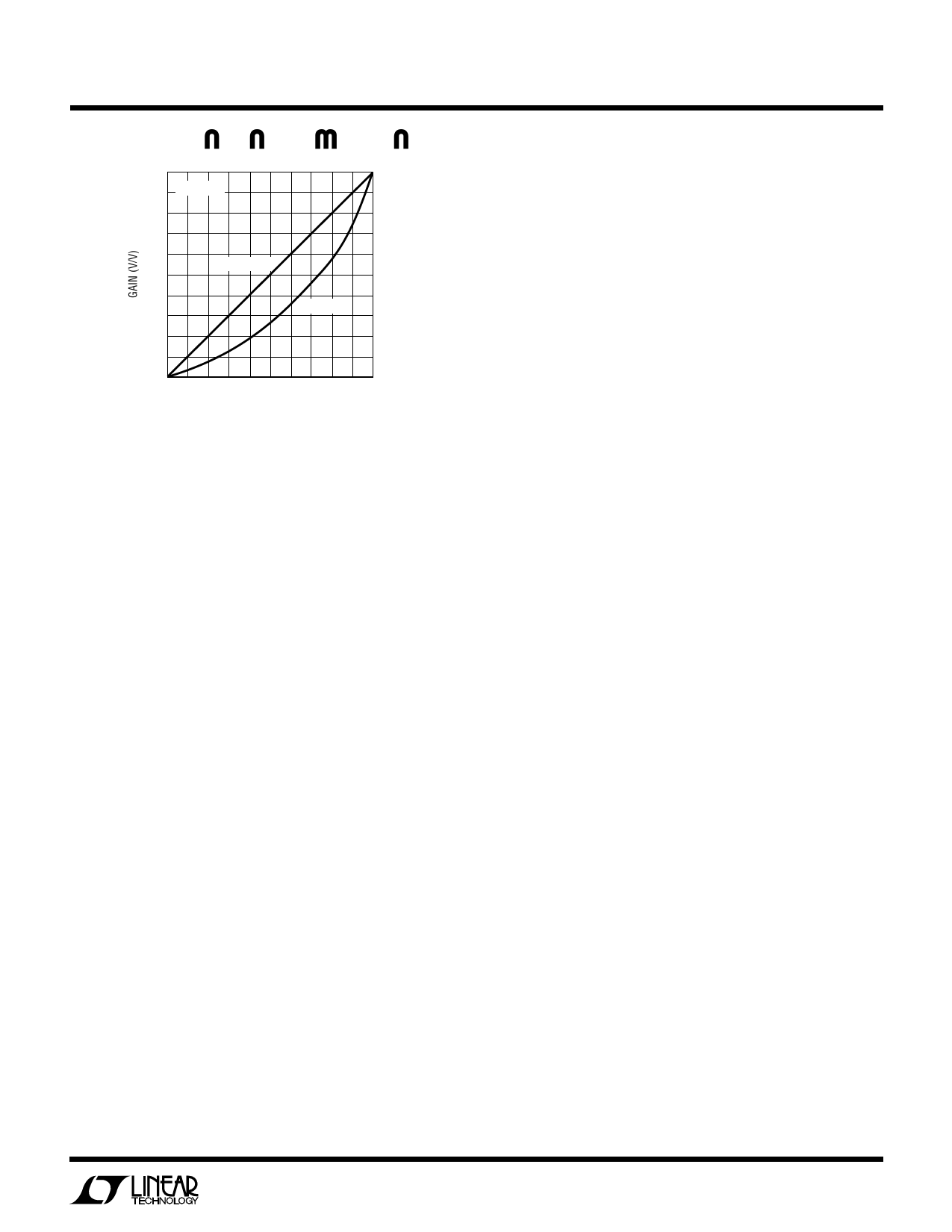
100
VFS = 2.5V
millivolts of the negative supply can drive the NULL pin.
The AM modulator application shows an LT1077 driving
the NULL pin to eliminate the output DC offset voltage.
RF2 = 4.3k
50
RF2 = 1.5k
0
0
0.5 1.0 1.5 2.0 2.5
CONTROL VOLTAGE (V)
1251/56 F01
Figure 1. Linear Gain Control from 0 to 101
Capacitive Loads
Increasing the value of the feedback resistor reduces the
bandwidth and open-loop gain of the LT1251/LT1256;
therefore, the pole introduced by a capacitive load can be
overcome. If there is little or no resistive load in parallel
with the load capacitance, the output stage will resonate,
peak and possibly oscillate. With a resistive load of 150Ω,
any capacitive load can be accommodated by increasing
the feedback resistor. If the capacitive load cannot be
paralleled with a DC load of 150Ω, a network of 200pF in
series with 100Ω should be placed from the output to
ground. Then the feedback resistor should be selected for
best response.
The Null Pin
Pin 6 can be used to adjust the gain of an internal current
mirror to change the output offset. The open circuit
voltage at Pin 6 is set by the full scale current IFS flowing
through 200Ω to the negative supply. Therefore, the NULL
pin sits 100mV above the negative supply with VFS equal
to 2.5V. Any op amp whose output swings within a few
Crosstalk
The amount of signal from the off input that appears at the
output is a function of frequency and the circuit topology.
The nature of a current feedback input stage is to force the
voltage at the inverting input to be equal to the voltage at
the noninverting input. This is independent of feedback
and forced by a buffer amplifier between the inputs. When
the LT1251/LT1256 are operating noninverting, the off
input signal is present at the inverting input. Since one end
of the feedback resistor is connected to this input, the off
signal is only a feedback resistor away from the output.
The amount of unwanted signal at the output is deter-
mined by the size of the feedback resistor and the output
impedance of the LT1251/LT1256. The output impedance
rises with increasing frequency resulting in more crosstalk
at higher frequencies. Additionally, the current that flows
in the inverting input is diverted to the supplies within the
chip and some of this signal will also show up at the
output. With a 1.5k feedback resistor, the crosstalk is
down about 86dB at low frequencies and rises to – 78dB
at 1MHz and on to – 60dB at 6MHz. The curves show the
details.
Distortion
When only one input is contributing to the output (VC = 0%
or 100%) the LT1251/LT1256 have very low distortion. As
the control reduces the output, the distortion will increase.
The amount of increase is a function of the current that
flows in the inverting input. Larger input signals generate
more distortion. Using a larger feedback resistor will
reduce the distortion at the expense of higher output
noise.
11
Share Link: 