HD74LVC2G66CPE 데이터 시트보기 (PDF) - Renesas Electronics
부품명
상세내역
일치하는 목록
HD74LVC2G66CPE Datasheet PDF : 12 Pages
| |||
HD74LVC2G66
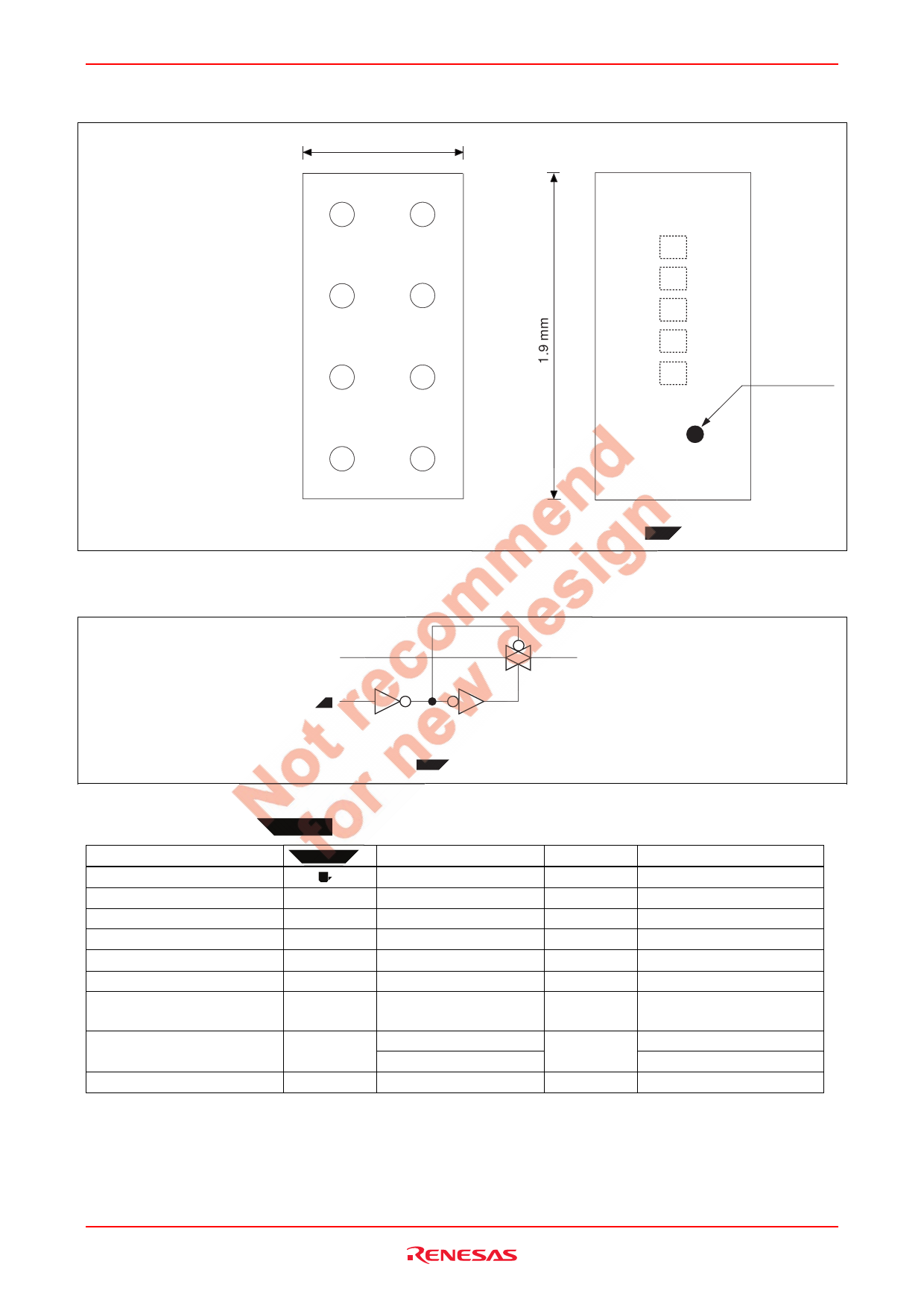
Pin Arrangement
Height 0.5 mm
0.5 mm pitch
0.17 mm 8–Ball (CP)
0.23 mm 8–Ball (CL)
GND
CONT2
0.9 mm
45
36
IN/OUT2
OUT/IN2
OUT/IN1
27
CONT1
Pin#1 INDEX
IN/OUT1
18
VCC
Logic Diagram
(Bottom view)
(Top view)
IN/OUT1
CONT1
OUT/IN1
one of two switches
Absolute Maximum Ratings
Item
Symbol
Ratings
Unit
Test Conditions
Supply voltage range
Input voltage range *1
Output voltage range *1, 2
Input clamp current
Output clamp current
Continuous output current
Continuous current through
VCC or GND
Package Thermal impedance
VCC
VI
VO
IIK
IOK
IO
ICC or IGND
θja
–0.5 to 6.5
–0.5 to 6.5
–0.5 to VCC +0.5
–50
–50
±50
±100
140
102
V
V
V
mA
mA
mA
mA
°C/W
Output : H or L
VI < 0
VO < 0
VO = 0 to VCC
CP
CL
Storage temperature
Tstg
–65 to 150
°C
Notes:
The absolute maximum ratings are values, which must not individually be exceeded, and furthermore no two
of which may be realized at the same time.
1. The input and output voltage ratings may be exceeded if the input and output clamp-current ratings are
observed.
2. This value is limited to 5.5 V maximum.
Rev.3.00 Jul 07, 2005 page 2 of 11
Share Link: 