HD74LV166A 데이터 시트보기 (PDF) - Renesas Electronics
부품명
상세내역
일치하는 목록
HD74LV166A Datasheet PDF : 10 Pages
| |||
HD74LV166A
Preliminary
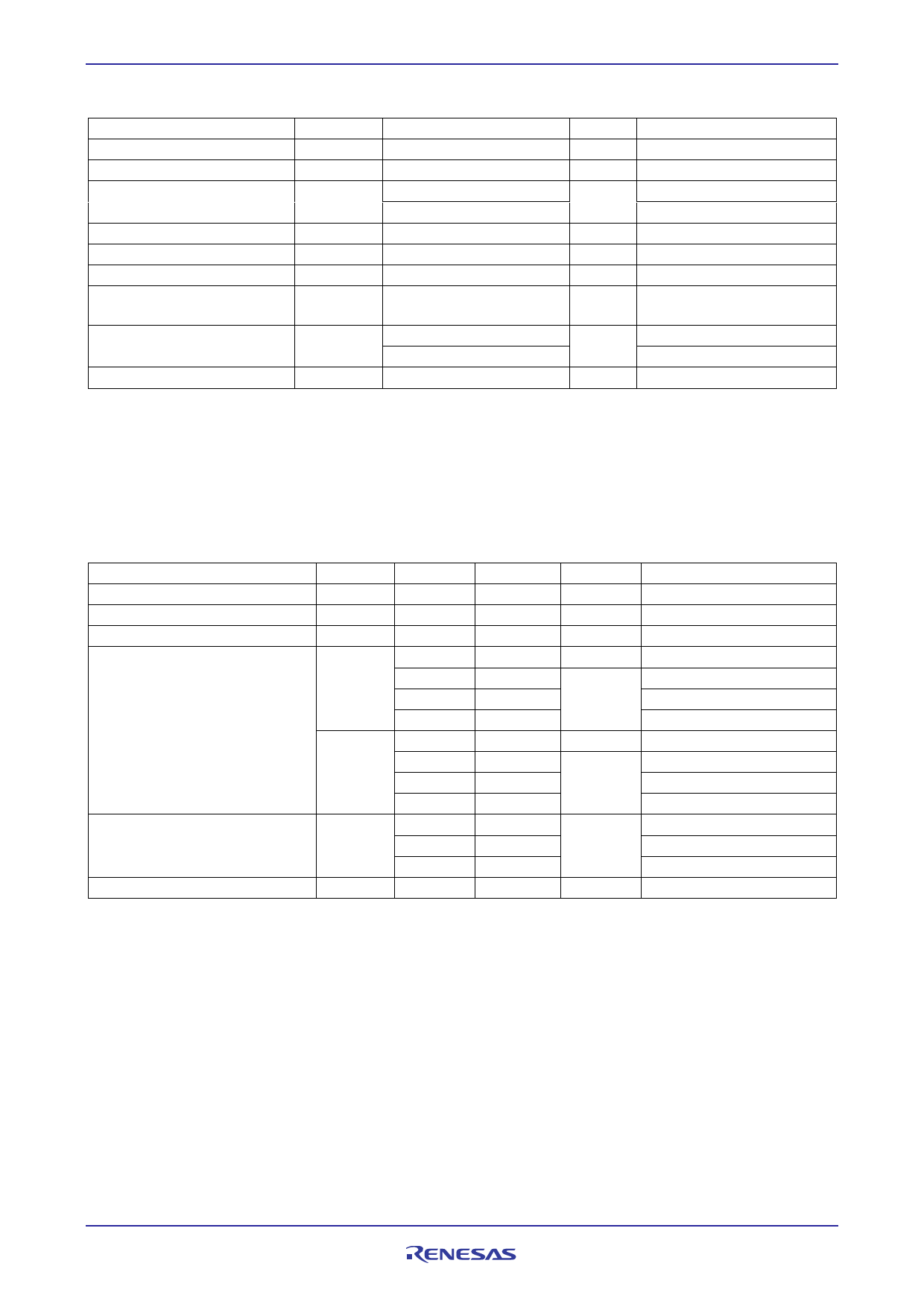
Absolute Maximum Ratings
Item
Symbol
Ratings
Unit
Conditions
Supply voltage range
VCC
Input voltage range*1
VI
Output voltage range*1, 2
VO
Input clamp current
Output clamp current
Continuous output current
Continuous current through
VCC or GND
Maximum power dissipation at
Ta = 25°C (in still air)*3
IIK
IOK
IO
ICC or IGND
PT
–0.5 to 7.0
–0.5 to 7.0
–0.5 to VCC + 0.5
–0.5 to 7.0
–20
±50
±25
±50
785
500
V
V
V
Output: H or L
VCC: OFF
mA VI < 0
mA VO < 0 or VO > VCC
mA VO = 0 to VCC
mA
mW SOP
TSSOP
Storage temperature
Tstg
–65 to 150
°C
Notes: The absolute maximum ratings are values, which must not individually be exceeded, and furthermore, no two of
which may be realized at the same time.
1. The input and output voltage ratings may be exceeded if the input and output clamp-current ratings are
observed.
2. This value is limited to 5.5 V maximum.
3. The maximum package power dissipation was calculated using a junction temperature of 150°C.
Recommended Operating Conditions
Item
Symbol
Min
Supply voltage range
Input voltage range
Output voltage range
Output current
VCC
2.0
VI
0
VO
0
IOH
—
—
—
—
IOL
—
—
—
—
Input transition rise or fall rate
t /v
0
0
0
Operating free-air temperature
Ta
–40
Note: Unused or floating inputs must be held high or low.
Max
5.5
5.5
VCC
–50
–2
–6
–12
50
2
6
12
200
100
20
85
Unit
V
V
V
A
mA
A
mA
ns/V
°C
Conditions
H or L
VCC = 2.0 V
VCC = 2.3 to 2.7 V
VCC = 3.0 to 3.6 V
VCC = 4.5 to 5.5 V
VCC = 2.0 V
VCC = 2.3 to 2.7 V
VCC = 3.0 to 3.6 V
VCC = 4.5 to 5.5 V
VCC = 2.3 to 2.7 V
VCC = 3.0 to 3.6 V
VCC = 4.5 to 5.5 V
R04DS0002EJ0400 Rev.4.00
Aug 16, 2010
Page 3 of 9
Share Link: 