HD74LVC1G02CPE 데이터 시트보기 (PDF) - Renesas Electronics
부품명
상세내역
일치하는 목록
HD74LVC1G02CPE Datasheet PDF : 9 Pages
| |||
HD74LVC1G02
2–input NOR Gate
Description
REJ03D0008–0300Z
Rev.3.00
Jun. 30, 2004
The HD74LVC1G02 has two–input NOR gate in a 5-pin package. Low voltage and high-speed operation is suitable for
the battery powered products (e.g., notebook computers), and the low power consumption extends the battery life.
Features
• The basic gate function is lined up as renesas uni logic series.
• Supply voltage range : 1.65 to 5.5 V
Operating temperature range: –40 to +85°C
• All inputs: VIH (Max.) = 5.5 V (@VCC = 0 V to 5.5 V)
All outputs: VO (Max.) = 5.5 V (@VCC = 0 V)
• Output current:
±4 mA (@VCC = 1.65 V)
±8 mA (@VCC = 2.3 V)
±24 mA (@VCC = 3.0 V)
±32 mA (@VCC = 4.5 V)
• Ordering Information
Part Name
Package Type
Package Code
HD74LVC1G02CPE
HD74LVC1G02CLE
WCSP-5 pin
TBS-5V
TBS-5AV
Package
Abbreviation
CP
CL
Taping Abbreviation
(Quantity)
E (3,000 pcs/reel)
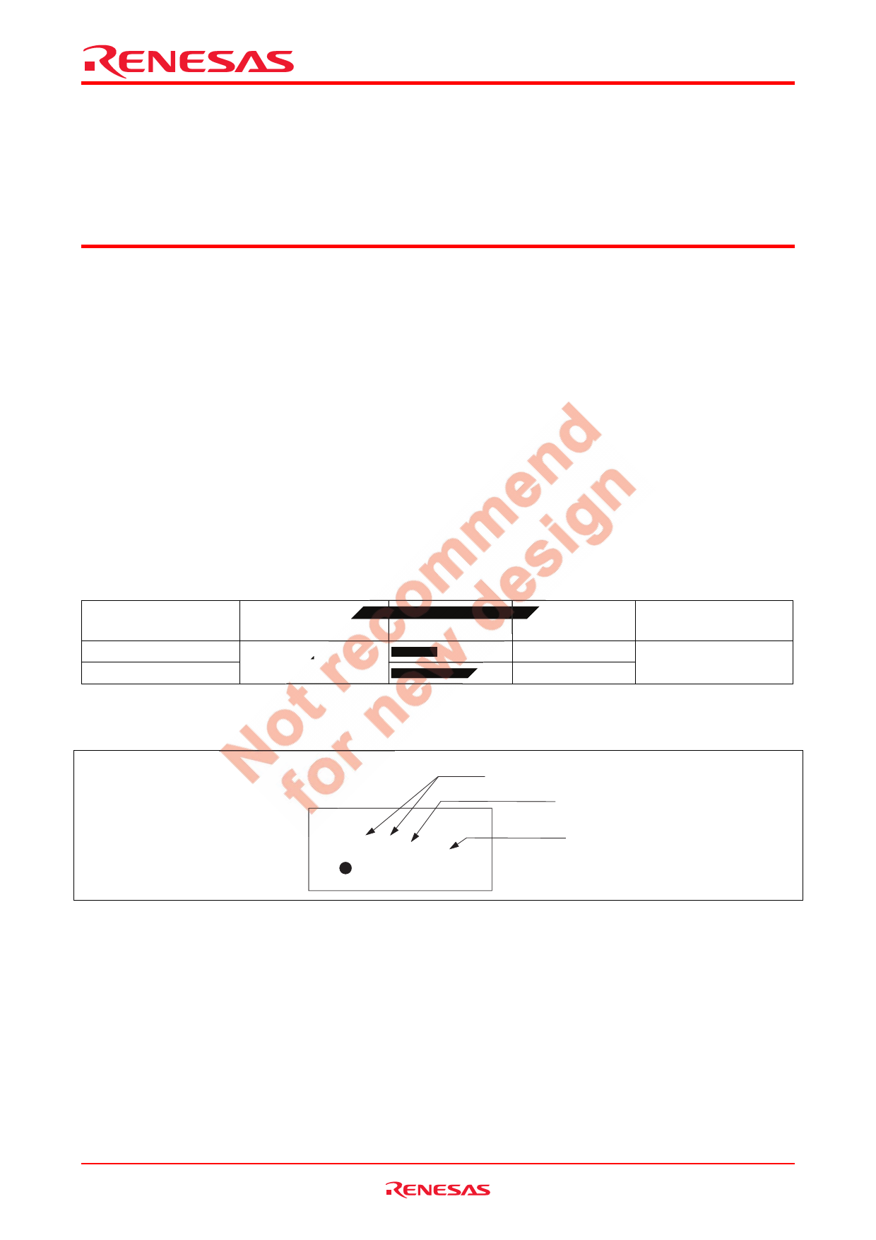
Article Indication
Marking
Year code
E3YM
Month code
Rev.3.00 Jun. 30, 2004 page 1 of 8
Share Link: 