HD74HCT688FPEL 데이터 시트보기 (PDF) - Renesas Electronics
부품명
상세내역
일치하는 목록
HD74HCT688FPEL Datasheet PDF : 8 Pages
| |||
HD74HCT688
Recommended Operating Conditions
Item
Symbol
Ratings
Supply voltage
VCC
4.5 to 5.5
Input / Output voltage
VIN, VOUT
0 to VCC
Operating temperature
Input rise / fall time*1
Ta
–40 to 85
tr, tf
0 to 500
Notes: 1. This item guarantees maximum limit when one input switches.
Waveform: Refer to test circuit of switching characteristics.
Unit
V
V
°C
ns
Conditions
VCC = 4.5 V
Electrical Characteristics
Item
Input voltage
Output voltage
Input current
Quiescent current
Symbol VCC (V)
VIH 4.5 to 5.5
VIL 4.5 to 5.5
VOH
4.5
4.5
VOL
4.5
4.5
Iin
5.5
ICC
5.5
Ta = 25°C
Min Typ Max
2.0 — —
— — 0.8
4.4 — —
4.18 — —
— — 0.1
— — 0.26
— — ±0.1
— — 4.0
Ta = –40 to+85°C
Min
Max
2.0
—
—
0.8
4.4
—
4.13
—
—
0.1
—
0.33
—
±1.0
—
40
Unit
V
V
V
V
µA
µA
Test Conditions
Vin = VIH or VIL IOH = –20 µA
IOH = –4 mA
Vin = VIH or VIL IOL = 20 µA
IOL = 4 mA
Vin = VCC or GND
Vin = VCC or GND, Iout = 0 µA
Switching Characteristics
Item
Propagation delay
time
Output rise/fall time
Input capacitance
Symbol
tPLH
tPHL
tPLH
tPHL
tTLH
tTHL
Cin
VCC (V)
4.5
4.5
4.5
4.5
4.5
—
Ta = 25°C
Min Typ Max
— 17 42
— 19 42
—
9
24
— 12 24
—
5
15
Ta = –40 to +85°C
Min Max
—
53
—
53
—
30
—
30
—
19
(CL = 50 pF, Input tr = tf = 6 ns)
Unit
Test Conditions
ns Por Q to output
ns Enable to output
ns
—
5
10
—
10
pF
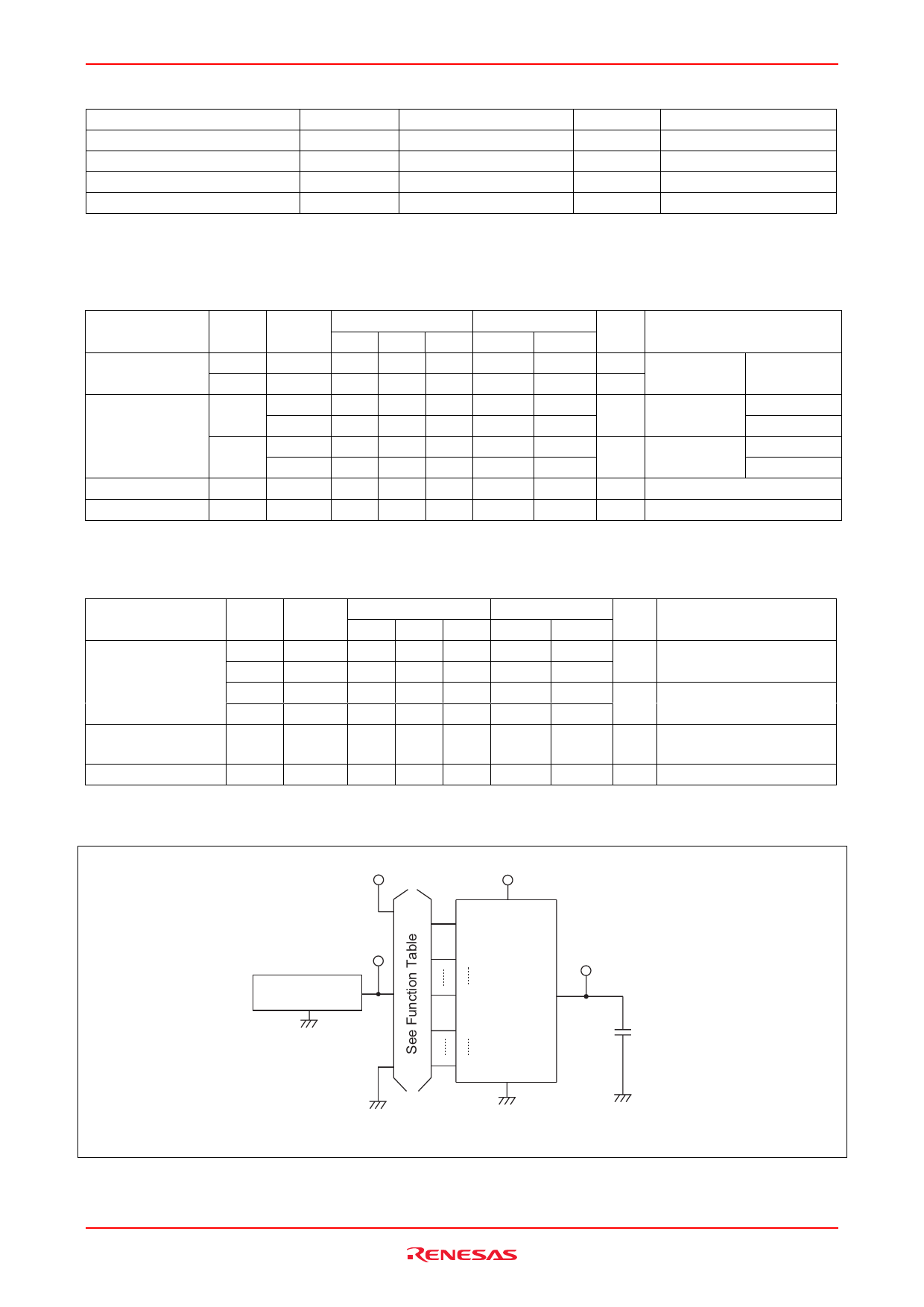
Test Circuit
VCC
VCC
Input
Pulse Generator
Zout = 50 Ω
G
P1
Output
P7
P=Q
Q0
Q7
CL =
50 pF
Note : 1. CL includes probe and jig capacitance.
Rev.2.00, Mar 30, 2006 page 4 of 7
Share Link: 