HD74HC95 데이터 시트보기 (PDF) - Renesas Electronics
부품명
상세내역
일치하는 목록
HD74HC95 Datasheet PDF : 7 Pages
| |||
HD74HC95
Switching Characteristics (CL = 50 pF, Input tr = tf = 6 ns)
Item
Maximum clock
frequency
Propagation delay
time
Pulse width
Setup time
Hold time
Output rise/fall
time
Input capacitance
Symbol VCC (V)
fmax
2.0
4.5
6.0
tPLH
2.0
4.5
6.0
tPHL
2.0
4.5
6.0
tw
2.0
4.5
6.0
tsu
2.0
4.5
6.0
th
2.0
4.5
6.0
tTLH, tTHL 2.0
4.5
6.0
Cin
—
Ta = 25°C
Ta = –40 to +85°C
Min Typ Max Min Max Unit
Test Conditions
—— 4
—
3 MHz
— — 20
—
16
— — 24
—
19
— — 145 —
180 ns
— 17 29
—
36
— — 25
—
31
— — 170 —
215 ns
— 17 34
—
43
— — 29
—
37
80 — — 100
— ns Clock
16 6 —
20
—
14 — —
17
—
100 — — 125
— ns
20 2 —
25
—
17 — —
21
—
10 — —
10
— ns
10 –1 —
10
—
10 — —
10
—
— — 75
—
95 ns
— 5 15
—
19
— — 13
—
16
— 5 10
—
10 pF
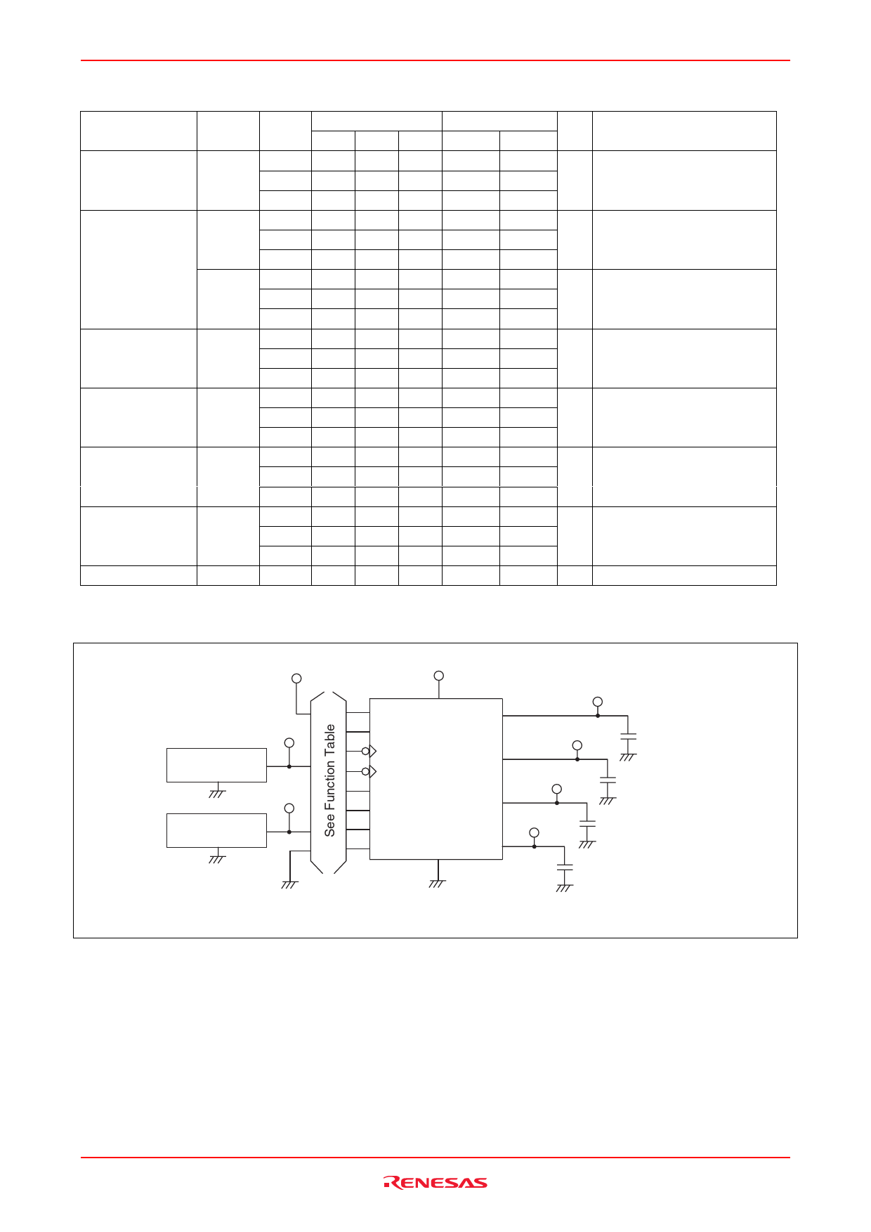
Test Circuit
VCC
Input
Pulse generator
Zout = 50 Ω
Input
Pulse generator
Zout = 50 Ω
VCC
Serial Input
Mode Control
Clock 1
Clock 2
A
B
C
D
Output
QA
Output
CL = 50 pF
QB
Output
CL = 50 pF
QC
Output
CL = 50 pF
QD
CL = 50 pF
Note: CL includes the probe and jig capacitance.
Rev.2.00, Oct 06, 2005 page 4 of 6
Share Link: 