HD74HC390 데이터 시트보기 (PDF) - Renesas Electronics
부품명
상세내역
일치하는 목록
HD74HC390 Datasheet PDF : 7 Pages
| |||
HD74HC390
Switching Characteristics (CL = 50 pF, Input tr = tf = 6 ns)
Item
Maximum clock
frequency
Propagation delay
time
Pulse width
Removal time
Output rise/fall
time
Input capacitance
Symbol VCC (V)
fmax
2.0
4.5
6.0
tPLH
2.0
tPHL
4.5
6.0
tPLH
2.0
tPHL
4.5
6.0
tPLH
2.0
tPHL
4.5
6.0
tPLH
2.0
tPHL
4.5
6.0
tPLH
2.0
tPHL
4.5
6.0
tPHL
2.0
4.5
6.0
tw
2.0
4.5
6.0
th
2.0
4.5
6.0
tTLH
2.0
tTHL
4.5
6.0
Cin
—
Ta = 25°C
Min Typ Max
——
5
— — 27
— — 32
— — 120
— 11 24
— — 20
— — 290
— 32 58
— — 49
— — 130
— 16 26
— — 22
— — 185
— 20 37
— — 31
— — 130
— 15 26
— — 22
— — 165
— 14 33
— — 28
80 — —
16 8 —
14 — —
25 — —
5
1—
4 ——
— — 75
— 5 15
— — 13
— 5 10
Ta = –40 to +85°C
Min
Max Unit
Test Conditions
—
4 MHz
—
21
—
25
—
150 ns Clock A to QA
—
30
—
26
—
365 ns Clock A to QC
—
73
(QA connected to Clock B)
—
62
—
165 ns Clock B to QB
—
33
—
28
—
230 ns Clock B to QC
—
46
—
39
—
165 ns Clock B to QD
—
33
—
28
—
205 ns Clear to QA, QB, QC, QD
—
41
—
35
100
—
ns
20
—
17
—
31
—
ns
6
—
5
—
—
95
ns
—
19
—
16
—
10 pF
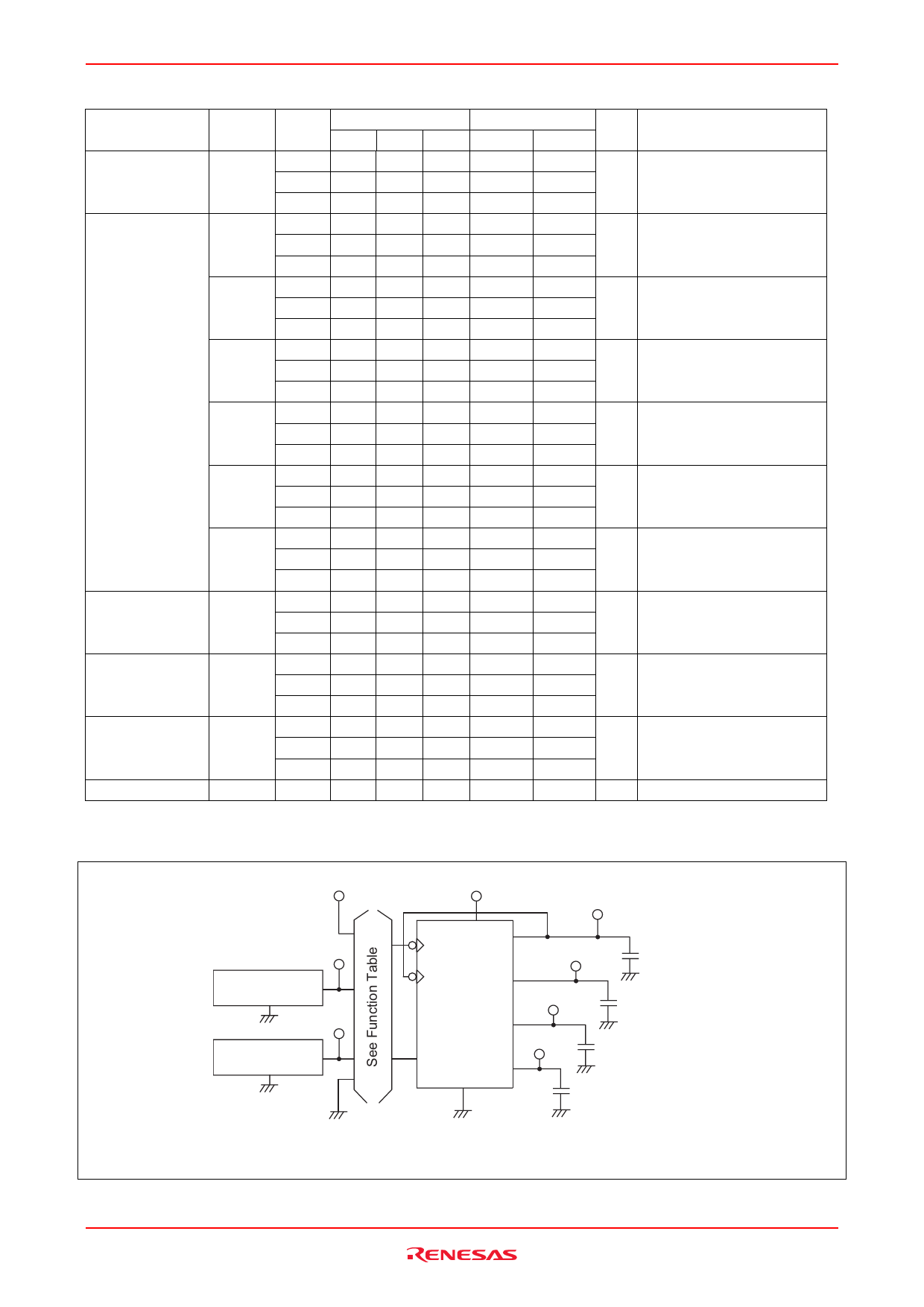
Test Circuit
VCC
Input
Pulse Generator
Zout = 50 Ω
Input
Pulse Generator
Zout = 50 Ω
VCC
Output
A
B
Clear
QA
Output
CL = 50 pF
QB
Output
QC
Output
QD
CL = 50 pF
CL = 50 pF
CL = 50 pF
Note : 1. CL includes probe and jig capacitance.
Rev.2.00 Mar 30, 2006 page 4 of 6
Share Link: 