HD74AC273RPEL 데이터 시트보기 (PDF) - Renesas Electronics
부품명
상세내역
일치하는 목록
HD74AC273RPEL Datasheet PDF : 8 Pages
| |||
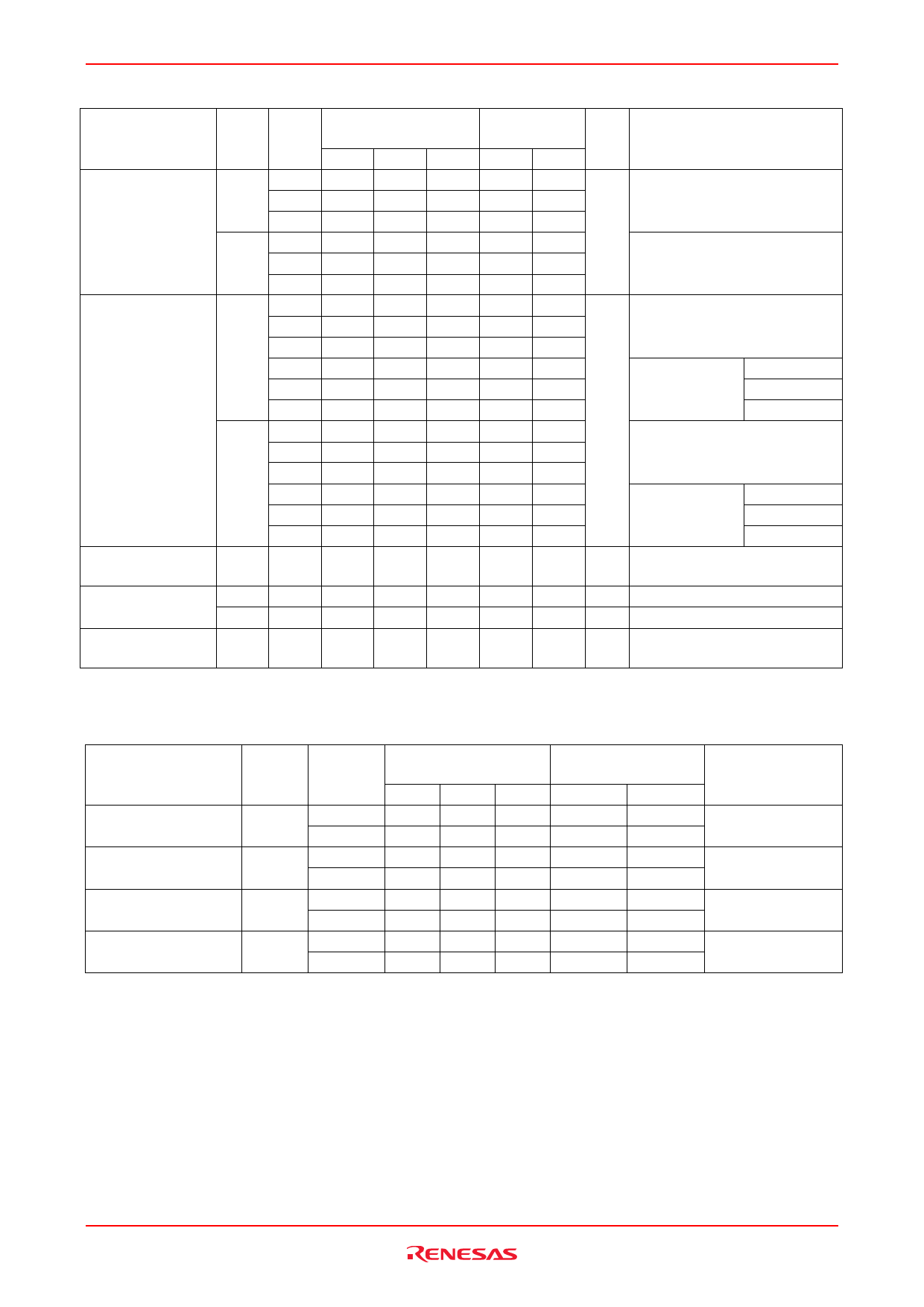
HD74AC273
DC Characteristics
Item
Sym- Vcc
bol (V)
Ta = 25°C
min. typ. max.
Input Voltage
VIH
3.0
2.1
1.5
—
4.5 3.15 2.25 —
5.5 3.85 2.75 —
VIL
3.0
—
4.5 —
1.50 0.9
2.25 1.35
5.5 —
2.75 1.65
Output voltage
VOH
3.0
2.9
2.99 —
4.5 4.4 4.49 —
5.5 5.4 5.49 —
3.0 2.58 —
—
4.5 3.94 —
—
5.5 4.94 —
—
VOL
3.0
—
4.5 —
0.002 0.1
0.001 0.1
5.5 —
0.001 0.1
3.0 —
—
0.32
4.5 —
—
0.32
5.5 —
—
0.32
Input leakage
current
IIN
5.5 —
—
±0.1
Dynamic output
IOLD
5.5
—
—
—
current*
IOHD
5.5
—
—
—
Quiescent supply ICC
5.5
—
—
8.0
current
*Maximum test duration 2.0 ms, one output loaded at a time.
Ta = –40 to
+85°C
min. max.
2.1 —
3.15 —
3.85 —
—
0.9
—
1.35
—
1.65
2.9 —
4.4 —
5.4 —
2.48 —
3.80 —
4.80 —
—
0.1
—
0.1
—
0.1
—
0.37
—
0.37
—
0.37
—
±1.0
86
—
–75 —
—
80
Unit
V
V
µA
mA
mA
µA
Condition
VOUT = 0.1 V or VCC –0.1 V
VOUT = 0.1 V or VCC –0.1 V
VIN = VIL or VIH
IOUT = –50 µA
VIN = VIL or VIH
VIN = VIL or VIH
IOUT = 50 µA
IOH = –12 mA
IOH = –24 mA
IOH = –24 mA
VIN = VIL or VIH IOL = 12 mA
IOL = 24 mA
IOL = 24 mA
VIN = VCC or GND
VOLD = 1.1 V
VOHD = 3.85 V
VIN = VCC or ground
AC Characteristics
Ta = +25°C
Ta = –40°C to +85°C
Item
Maximum clock
frequency
Symbol
fmax
VCC (V)*1
3.3
5.0
CL = 50 pF
Min Typ Max
90
125 —
140 175 —
CL = 50 pF
Min
Max
75
—
125
—
Unit
MHz
Propagation delay
tPLH
3.3
Clock to output
5.0
1.0 7.0 12.5 1.0
1.0 5.5 9.0 1.0
14.0
ns
10.0
Propagation delay
tPHL
3.3
Clock to output
5.0
1.0 7.0 13.0 1.0
1.0 5.0 10.0 1.0
14.5
ns
11.0
Propagation delay
tPHL
3.3
MR to output
5.0
1.0 7.0 13.0 1.0
1.0 5.0 10.0 1.0
14.0
ns
10.5
Note: 1. Voltage Range 3.3 is 3.3 V ± 0.3 V
Voltage Range 5.0 is 5.0 V ± 0.5 V
Rev.2.00, Jul.16.2004, page 4 of 7
Share Link: 