GS1582(2007) 데이터 시트보기 (PDF) - Gennum -> Semtech
부품명
상세내역
일치하는 목록
GS1582
(Rev.:2007)
(Rev.:2007)
Gennum -> Semtech

GS1582 Datasheet PDF : 114 Pages
| |||
GS1582 Data Sheet
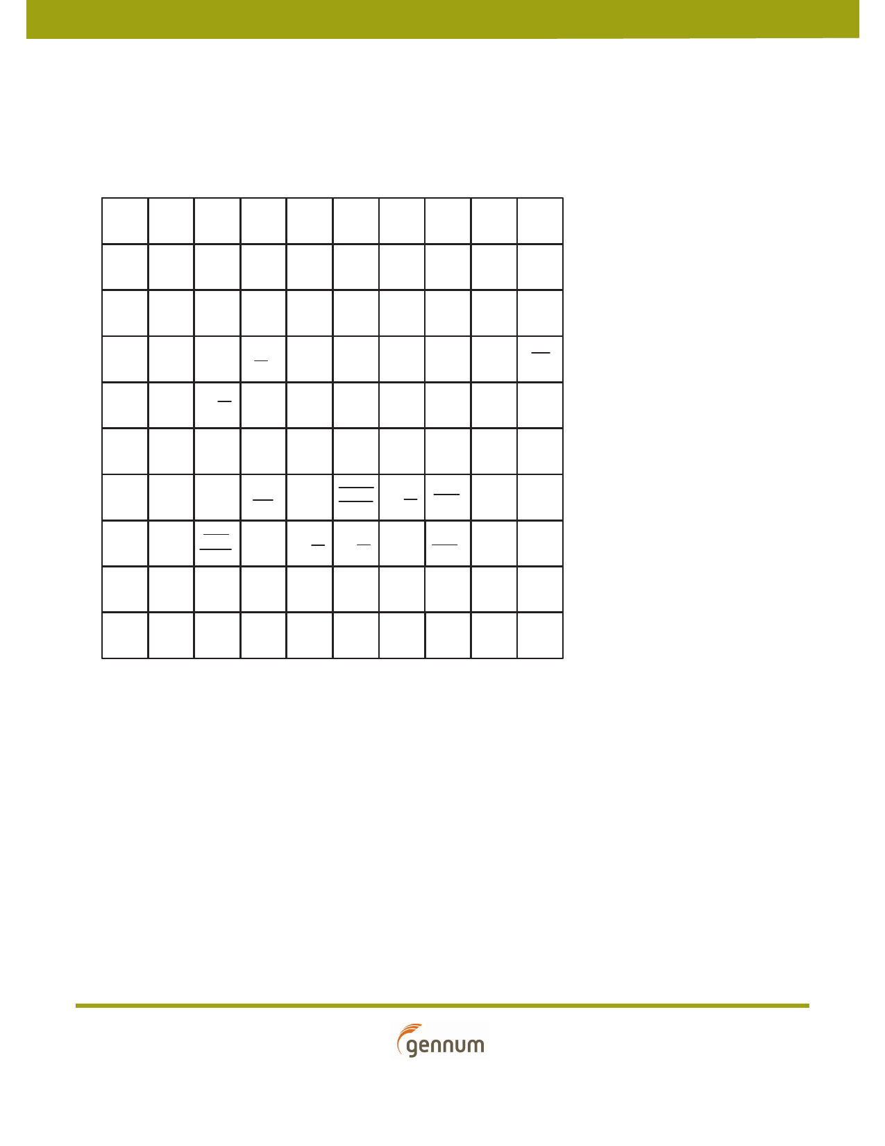
Table 1-1: Pin Descriptions (Continued)
Pin
Number
Name
Timing
Type Description
A3
A4
A5, E1, G10,
K8
A6, B6
A7
A8
A9
A10
F/DE
H/HSYNC
CORE_VDD
PD_VDD
LF
VCO_VCC
VCO
CP_VDD
Synchronous
with PCLK
Synchronous
with PCLK
Non
Synchronous
Analog
Analog
Analog
Analog
Analog
Input
Input
Input
Power
Input
Power
Input
Output
Power
Input
Input
Power
PARALLEL DATA TIMING
Signal levels are LVCMOS/LVTTL compatible.
TIM_861 = LOW:
Used to indicate the ODD / EVEN field of the video signal when
DETECT_TRS is set LOW. The device will set the F bit in all outgoing
TRS signals for the entire period that the F input signal is HIGH
(IOPROC_EN/DIS must also be HIGH).
The F signal should be set HIGH for the entire period of field 2 and
should be set LOW for all lines in field 1 and for all lines in progressive
scan systems.
The F signal is ignored when DETECT_TRS = HIGH.
TIM_861 = HIGH:
The DE signal is used to indicate the active video period. DE is HIGH for
active data and LOW for blanking. See Section 4.3.1 and Section 4.3.2
for timing details.
The DE signal is ignored when DETECT_TRS = HIGH.
PARALLEL DATA TIMING
Signal levels are LVCMOS/LVTTL compatible.
TIM_861 = LOW:
The H signal is used to indicate the portion of the video line containing
active video data, when DETECT_TRS is set low.
Active Line Blanking
The H signal should be set HIGH for the entire horizontal blanking
period, including the EAV and SAV TRS words, and LOW otherwise.
This is the default setting.
TRS Based Blanking (H_CONFIG = 1h)
The H signal should be set HIGH for the entire horizontal blanking
period as indicated by the H bit in the received TRS ID words, and LOW
otherwise.
The H signal is ignored when DETECT_TRS = HIGH.
TIM_861 = HIGH:
The HSYNC signal indicates horizontal timing. See Section 4.3.1 for
timing details.
The HSYNC signal is ignored when DETECT_TRS = HIGH.
Power supply connection for the digital core logic. Connect to +1.8V DC
digital.
Power supply connection for the phase detector. Connect to +1.8V DC
analog.
PLL loop filter connection.
Power supply for the external voltage controlled oscillator.
2.5V DC supplied by the device to the external VCO.
Input from external VCO.
Power supply connection for the charge pump and on chip VCO
regulator. Connect to +3.3V DC analog.
40117 - 1 November 2007
9 of 114
Share Link: