GM6605-1.5TA3R 데이터 시트보기 (PDF) - Gamma Microelectronics Inc.
부품명
상세내역
일치하는 목록
GM6605-1.5TA3R Datasheet PDF : 10 Pages
| |||
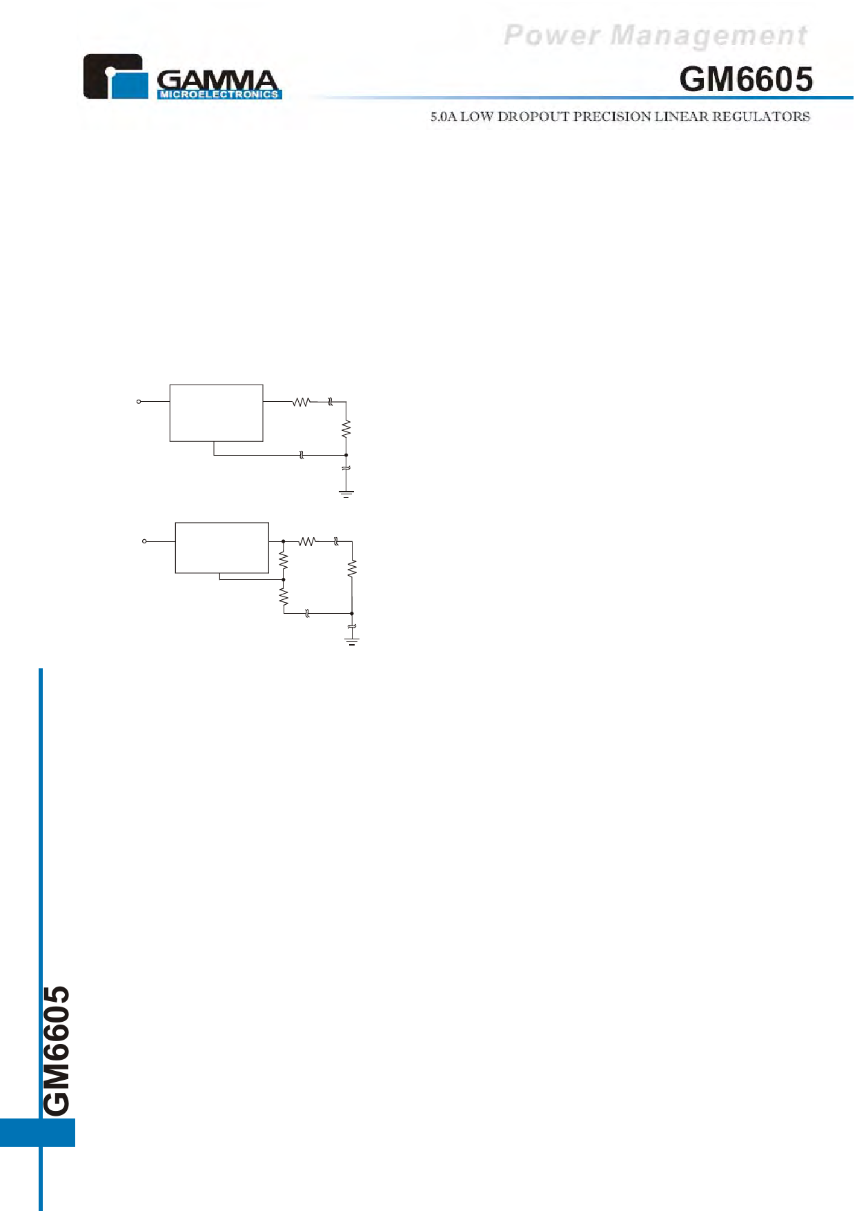
Output Voltage Sensing
GM6605 series is three terminal regulator, so they can-
not provide true remote load sensing. Load regulation
is limited by the resistance of the conductors connect-
ing the regulator to the load. For best results, Gm6605
should be connected as shown in Figure 2.
VIN
VIN
VOUT
GM6605-3.3
GND
Conductor
Parasitic
RC
Resistance
RLOAD
(a) Fixed Version
VIN
VIN
VOUT
RC
GM6605-A
ADJ
R1
R2
(b) Adjustable Version
Conductor
Parasitic
Resistance
RLOAD
(a),(b)
Figure 2 Conductor Parasitic Resistance Effects are
Minimized by this Grounding Scheme For Fixed
and Adjustable Output Regulators
Calculating Power Dissipation and Heat
Sink Requirements
GM6605 series precision linear regulators include ther-
mal shutdown and current limit circuitry to protect the
devices. However, high power regulators normally oper-
ate at high junction temperatures so it is important to
calculate the power dissipation and junction tempera-
tures accurately to be sure that you use and adequate
heat sink. The case is connected to VOUT on GM6605.
so electrical isolation may be required for some appli-
cations. Thermal compound should always be used
with high current regulators like GM6605.
The thermal characteristics of an IC depend on four
factors:
1. Maximum Ambient Temperature TA (°C)
2. Power Dissipation PD (Watts)
3. Maximum Junction Temperature TJ (°C)
4. Thermal Resistance Junction to ambient RQJA
(°C/W)
These relationship of these four factors is expressed
by equation (1):
TJ = TA + PD X RQJA ........(1)
Maximum ambient temperature and power dissipa-
tion are determined by the design while the maximum
junction temperature and thermal resistance depend
on the manufacturer and the package type.
The maximum power dissipation for a regulator is ex-
pressed by equation (2):
PD(max) = { VIN(max)- VOUT(min) } IOUT(max) + VIN(max)IQ ........(2)
where:
VIN(max) is the maximum input voltage,
VOUT(min) is the minimum output voltage,
IOUT(max) is the maximum output current
IQ is the maximum quiescent current at IOUT(max).
A heat sink effectively increases the surface area of
the package to improve the flow of heat away from
the IC into the air. Each material in the heat flow path
between the IC and the environment has a thermal re-
sistance. Like series electrical resistances, these re-
, sistance are summed to determine RQJA the total
thermal resistance between the junction and the air.
This is expressed by equation (3):
RQJA = RQJC + RQCS+ RQSA ........(3)
Where all of the following are in °C/W:
RQJC is thermal resistance of junction to case,
RQCS is thermal resistance of case to heat sink,
RQSA is thermal resistance of heat sink to ambient air
The value for RQJA is calculated using equation (3)
and the result can be substituted in equation (1). The
value for RQJC is 3.5°C/W for a given package type
based on an average die size. For a high current reg-
ulator such as GM6605, the majority of the heat is
generated in the power transistor section.
6
Share Link: 