NJG1705V-C2 데이터 시트보기 (PDF) - Japan Radio Corporation
부품명
상세내역
일치하는 목록
NJG1705V-C2 Datasheet PDF : 26 Pages
| |||
NJG1705V
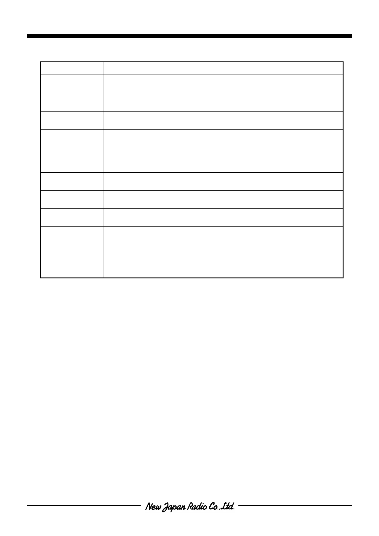
nTERMINAL INFORMATION
No. SYMBOL
DESCRIPTIONS
1
LNAIN
RF input terminal of LNA. The RF signal is input through external matching
circuit.
2
LNACAP
Terminal for the bypass capacitor of LNA. The bypass capacitor C1 shown in
application circuit, should be connected to this terminal as close as possible.
3
GND Ground terminal(0V)
IF signal output terminal. The IF signal is output though external matching
4
IFOUT circuit’s connected to this terminal. Please connect inductance L8 and power
supply as application circuit since it is also the terminal of Mixer power supply.
5
VLO
Power supply terminal for local amplifier. Please connect R1 and L10 to this
terminal shown in the application circuit as close as possible.
6
LOIN
Local signal input terminal of local amplifier. The local signal is terminal to
local amplifier through external matching circuit.
7
GND Ground terminal(0V)
8
MIXIN
RF signal input terminal of Mixer. The RF signal from LNA is sent to Mixer
through matching circuit.
9
GND Ground terminal(0V)
Signal output terminal of LNA. The RF signal from LNA is output through
10
LNAOUT
external matching circuit connected to this terminal. Please connect
inductance L4 and power supply shown in application circuit, since it is also
the terminal of LNA power supply.
CAUTION
1) Ground terminal (No.3, 7, 9) should be connected to the ground plane as short as possible.
-6-
Share Link: 