G5111T12 데이터 시트보기 (PDF) - Global Mixed-mode Technology Inc
부품명
상세내역
일치하는 목록
G5111T12 Datasheet PDF : 8 Pages
| |||
Global Mixed-mode Technology Inc.
G5111
Capacitor Selection
Low ESR (Equivalent Series Resistance) capacitors
should be used at the output to minimize the output
ripple voltage and the peak-to-peak transient voltage.
Multilayer ceramic capacitors (MLCC) are the best
choice, as they have a very low ESR and are available
in very small packages. Their small size makes them a
good match with the G5111’s SOT-23-5 package. If
solid tantalum capacitors (like the AVX TPS, Sprague
593D families) or OS-CON capacitors are used, they
will occupy more volume than a ceramic ones and the
higher ESR increases the output ripple voltage. Notice
that use a capacitor with a sufficient voltage rating.
A low ESR surface-mount ceramic capacitors also
make a good selection for the input bypass capacitor,
which should be placed as close as possible to the
G5111. A 4.7µF input capacitor is sufficient for most
applications.
Diode Selection
For most G5111 applications, the high switching fre-
quency requires a high-speed rectifier Schottky diodes,
such as the Motorola MBR0530 (0.5A, 30V) with their
low forward voltage drop and fast switching speed, are
recommended. Many different manufacturers make
equivalent parts, but make sure that the component is
rated to operate at least 0.35A. To achieve high effi-
ciency, the average current rating of the Schottky di-
odes should be greater than the peak switching cur-
rent. Choose a reverse breakdown voltage greater
than the output voltage.
Lowering Output Voltage Ripple
The G5111 supplies energy to the load in bursts by
ramping up the inductor current, then delivering that
current to the load. To use low ESR capacitors will
help minimize the output ripple voltage, but proper
selection of the inductor and the output capacitor also
plays a big role. If a larger inductance value or a
smaller capacitance value is used, the output ripple
voltage will increase because the capacitor will be
slightly overcharged each burst cycle. To reduce the
output ripple, increase the output capacitance value or
add a 10pF feed-forward capacitor in the feedback
network of the G5111 (see the circuits in the Typical
Applications section). To add this small, inexpensive
10pF capacitor will greatly reduce the output voltage
ripple.
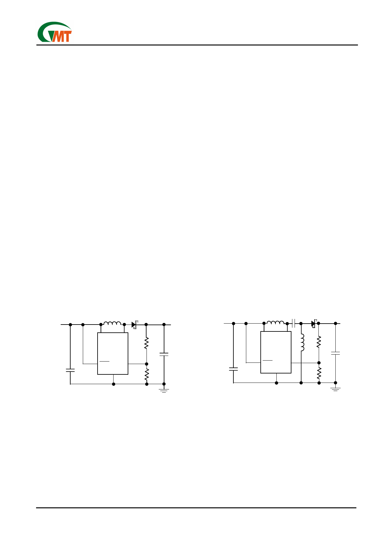
Typical Applications
Boost Converter
SEPIC Converter
VIN
2.5V to 4.2V
C1
4.7µF
L1
4.7µH
D1
VCC
SW
G5111
SHDN
FB
GND
5V
50mA
R1
390k
C2
22µF
R2
120k
L1:MURATA LQH3C4R7M24
D1:MOTOROLA MBR0520
VIN
2.5V to 4.2V
C1
4.7µF
C3
L1
10µH
1µF
D1
VCC
SW
G5111
SHDN
FB
GND
L2
10µH
R1
470k
R2
270k
3.3V
60mA
C2
22µF
L1,L2:MURATA LQH3C100K24
D1:MOTOROLA MBR0520
Ver: 1.2
Sep 09, 2004
TEL: 886-3-5788833
http://www.gmt.com.tw
6
Share Link: 