FX-500-LAF-NNK-D7-J1 데이터 시트보기 (PDF) - Vectron International
부품명
상세내역
일치하는 목록
FX-500-LAF-NNK-D7-J1 Datasheet PDF : 6 Pages
| |||
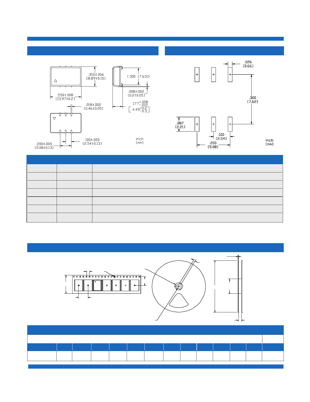
Outline Diagram
654
FX-500-LAC-GNK
8K000/77M760
VI 142
1 23
FX-500 Low Jitter Frequency Translator
Pad Layout
Pin Out
Pin #
1
2
3
4
5
6
Symbol
fIN
Tri-state1
GND
Fo
LD2
VDD
Function
Input Frequency
Logic Low = Output Disable / Logic High = Output Enabled
Case and Electrical Ground
Output Frequency
Lock Detect
Power Supply Voltage (3.3 V ± 0.3 or 5.0 V ± 0.5)
1. Tristate is driven to logic high or logic low; there is no internal pull up or pull down resistor.
2. LD is an open collector output requiring a 30k ohm pullup resistor to VDD. LD output is logic high under locked condition, logic
low for no input at fIN, and for "out-of-lock" condition LD transitions between logic low and logic high at the phase detector frequency.
Tape and Reel
D
C
G
J
F
B
A
L
I
E
H
Tape and Reel Dimensions (mm)
Tape Dimensions
Reel Dimensions
Product A
B
C
D
E
F
GH
I
FX-500 24 11.5 1.5
4
12 1.78 21 13 100
K
# Per Reel
J
KL
5
25 330 200
Vectron International • 267 Lowell Road, Hudson, NH 03051 • Tel: 1-88-VECTRON-1 • Web: www.vectron.com
3
Share Link: 