SN54LS194A 데이터 시트보기 (PDF) - Motorola => Freescale
부품명
상세내역
일치하는 목록
SN54LS194A Datasheet PDF : 6 Pages
| |||
SN54 / 74LS194A
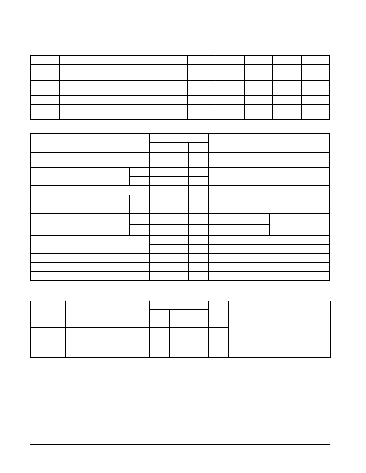
GUARANTEED OPERATING RANGES
Symbol
Parameter
VCC
Supply Voltage
TA
Operating Ambient Temperature Range
IOH
Output Current — High
IOL
Output Current — Low
Min
Typ
Max
Unit
54
4.5
5.0
5.5
V
74
4.75
5.0
5.25
54
– 55
25
125
°C
74
0
25
70
54, 74
– 0.4
mA
54
4.0
mA
74
8.0
DC CHARACTERISTICS OVER OPERATING TEMPERATURE RANGE (unless otherwise specified)
Limits
Symbol
Parameter
Min Typ Max Unit
Test Conditions
VIH
Input HIGH Voltage
2.0
Guaranteed Input HIGH Voltage for
V All Inputs
54
VIL
Input LOW Voltage
74
0.7
Guaranteed Input LOW Voltage for
0.8
V All Inputs
VIK
VOH
Input Clamp Diode Voltage
– 0.65 – 1.5
V VCC = MIN, IIN = – 18 mA
Output HIGH Voltage
54
2.5
3.5
74
2.7
3.5
V VCC = MIN, IOH = MAX, VIN = VIH
V or VIL per Truth Table
VOL
Output LOW Voltage
54, 74
74
0.25 0.4
0.35 0.5
20
IIH
Input HIGH Current
0.1
IIL
Input LOW Current
– 0.4
IOS
Short Circuit Current (Note 1)
– 20
– 100
ICC
Power Supply Current
23
Note 1: Not more than one output should be shorted at a time, nor for more than 1 second.
V IOL = 4.0 mA
V IOL = 8.0 mA
VCC = VCC MIN,
VIN = VIL or VIH
per Truth Table
µA VCC = MAX, VIN = 2.7 V
mA VCC = MAX, VIN = 7.0 V
mA VCC = MAX, VIN = 0.4 V
mA VCC = MAX
mA VCC = MAX
AC CHARACTERISTICS (TA = 25°C)
Symbol
fMAX
tPLH
tPHL
tPHL
Parameter
Maximum Clock Frequency
Propagation Delay,
Clock to Output
Propagation Delay,
MR to Output
Limits
Min Typ Max
25
36
14
22
17
26
19
30
Unit
MHz
ns
ns
Test Conditions
VCC = 5.0 V
CL = 15 pF
FAST AND LS TTL DATA
5-362
Share Link: 