AN-8027 데이터 시트보기 (PDF) - Fairchild Semiconductor
부품명
상세내역
일치하는 목록
AN-8027 Datasheet PDF : 17 Pages
| |||
AN-8027
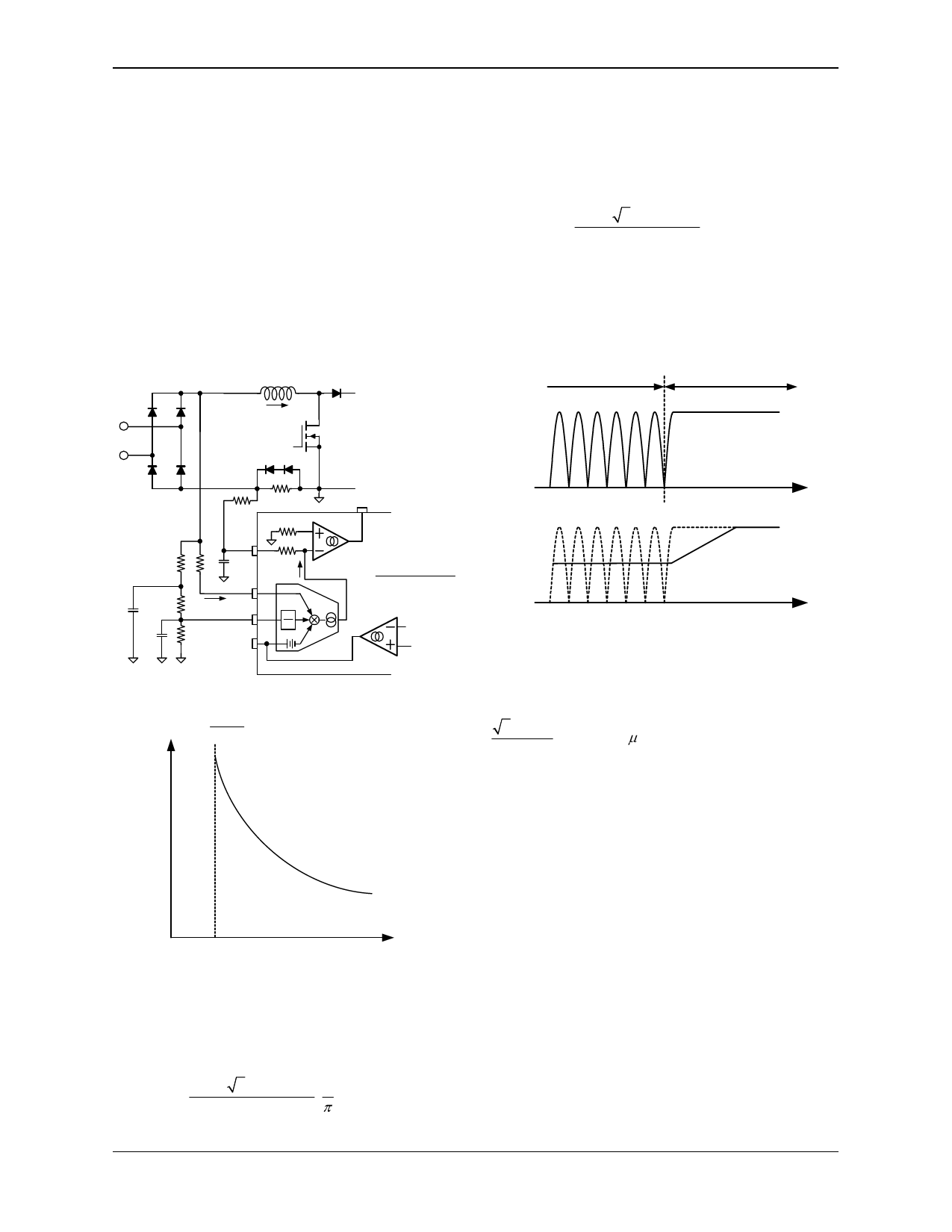
Functional Description
Gain Modulator
The gain modulator is the key block for PFC stage because
it provides the reference to the current control error
amplifier for the input current shaping, as shown in Figure
2. The output current of gain modulator is a function of VEA,
IAC , and VRMS. The gain of the gain modulator is given in
the datasheet as a ratio between IMO and IAC with a given
VRMS when VEA is saturated to HIGH. The gain is inversely
proportional to VRMS2, as shown in Figure 3, to implement
line feed-forward. This automatically adjusts the reference
of current control error amplifier according to the line
voltage such that the input power of PFC converter is not
changed with line voltage.
VIN
IL
However, once PFC stops switching operation, the junction
capacitance of bridge diode is not discharged and VIN of
Figure 2 is clamped at the peak of the line voltage. Then,
the voltage of VRMS pin is given by:
V NS
RMS
= VLINE
2RRMS 3
RRMS1 + RRMS 2 + RRMS 3
(2)
Therefore, the voltage divider for VRMS should be
designed considering the brownout protection trip point
and minimum operation line voltage.
PFC runs
VIN
PFC stops
ISENS
E
RRMS1
CRMS1
CRMS2
RIAC
RRMS2 IAC
IA
C
VRMS
RRMS3
VEA
IEA
R
M
R
IMO = G ⋅ IAC
M
=
IAC
⋅
K ⋅ (VEA − 0.7)
VRMS2 (VEAMAX − 0.7)
kx
2
Gain
Modulator
Figure 2. Gain Modulator Block
G∝ 1
VRMS 2
VRMS
VRMS-UVP
Figure 3. Modulation Gain Characteristics
To sense the RMS value of the line voltage, an averaging
circuit with two poles is typically employed, as shown in
Figure 2. The voltage of VRMS pin in normal PFC
operation is given as:
VRMS
Figure 4. VRMS According to the PFC Operation
The rectified sinusoidal signal is obtained by the current
flowing into the IAC pin. The resistor RIAC should be large
enough to prevent saturation of the gain modulator as:
2VLINE.BO ⋅ G MAX < 159μ A
(3)
RIAC
where VLINE.BO is the line voltage that trips brownout
protection, GMAX is the maximum modulator gain when VRMS
is 1.08V (which can be found in the datasheet), and 159µA is
the maximum output current of the gain modulator.
Current and Voltage Control of Boost Stage
As shown in Figure 5, the FAN480X employs two control
loops for power factor correction: a current control loop
and a voltage control loop. The current control loop shapes
inductor current, as shown in Figure 6, based on the
reference signal obtained at the IAC pin as:
IL ⋅ RCS1 = IMO ⋅ RM = I AC ⋅ G ⋅ RM
(4)
VRMS
= VLINE
2RRMS 3
RRMS1 + RRMS 2 + RRMS 3
⋅2
π
where VLINE is RMS value of line voltage.
© 2009 Fairchild Semiconductor Corporation
Rev. 1.0.0 • 8/26/09
(1)
2
www.fairchildsemi.com
Share Link: 