FA5304AP 데이터 시트보기 (PDF) - Fuji Electric
부품명
상세내역
일치하는 목록
FA5304AP Datasheet PDF : 17 Pages
| |||
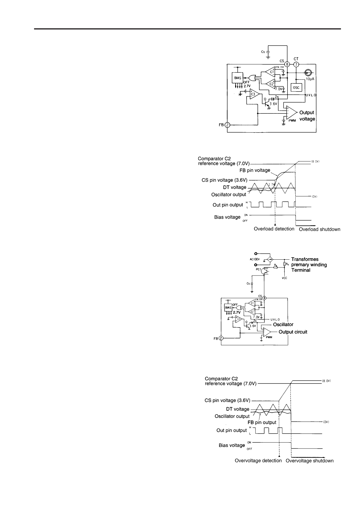
4.2 Overload shutdown
Figure 9 shows the overload shutdown circuit, and Figure 10 is
a timing chart which illustrates overload shutdown operation.If
the output voltage drops due to an overload or short-circuit, the
output voltage of the FB pin rises. If FB pin voltage exceeds
the reference voltage (2.7V) of comparator C3, the output of
comparator C3 switches low to turn transistor Q off. In normal
operation, transistor Q is on and the CS pin is clamped at 3.6V
by zener diode Zn. With Q off, the clamp is released and the
10µA constant-current source begins to charge capacitor CS
again and the CS pin voltage rises. When the CS pin voltage
exceeds the reference voltage (7.0V) of comparator C2, the
output of comparator C2 switches high to turn the bias circuit
off. The IC then enters the latched mode and shuts the output
down. Shutdown current consumption is 400µA(VCC=9V).
This current must be supplied through the startup resistor. The
IC then discharges the MOSFET gates.
Shutdown operation initiated by an overload can be reset by
lowering supply voltage VCC below 8.7V or forcing the CS pin
voltage below 7.0V.The period tOL from the time that the output
is short-circuited to the time that the bias circuit turns off is
given by the following equation:
tOL(mS) = 340Cs(µF).........................................(3)
4.3 Overvoltage shutdown
Figure 11 shows the overvoltage shutdown circuit, and Figure
12 is a timing chart which illustrates overvoltage shutdown
operation.
The optocoupler PC1 is connected between the CS and VCC
pins. If the output voltage rises too high, the PC1 turns on to
raise the voltage at the CS pin via resistor R6. When the CS
pin voltage exceeds the reference voltage (7.0V) of
comparator C2, comparator C2 switches high to turn the bias
circuit off. The IC then enters the latched mode and shuts the
output down. The shutdown current consumption of the IC is
400µA(VCC=9V). This current must be applied via startup
resistor R5.
The IC then discharges the MOSFET gates.
The shutdown operation initiated by an overvoltage condition
can be reset by lowering supply voltage VCC below 8.7V or
forcing the CS pin voltage below 7.0V.
During normal operation, the CS pin is clamped by a 3.6V
zener diode with a sink current of 150µA max. Therefore, a
current of 150µA or more must be supplied by the optocoupler
in order to raise the CS pin voltage above 7.0V.
FA5304AP(S)/FA5305AP(S)
Fig. 9 Overload shutdown circuit
Fig. 10 Overload shutdown timing chart
Fig. 11 Overvoltage shutdown circuit
Fig. 12 Overvoltage shutdown timing chart
7
Share Link: 