EN25F32 데이터 시트보기 (PDF) - Eon Silicon Solution Inc.
부품명
상세내역
일치하는 목록
EN25F32 Datasheet PDF : 40 Pages
| |||
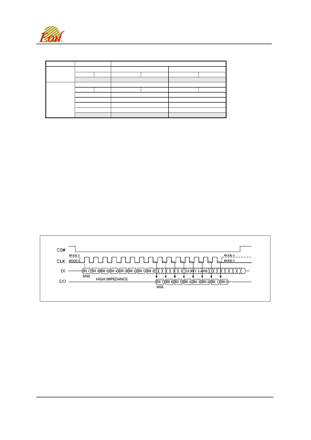
Table 2. Uniform Block Sector Architecture (End)
Block
1
0
Sector
31
16
15
4
3
2
1
0
Address range
01F000h
01FFFFh
010000h
00F000h
010FFFh
00FFFFh
004000h
003000h
002000h
001000h
000000h
004FFFh
003FFFh
002FFFh
001FFFh
000FFFh
EN25F32
OPERATING FEATURES
SPI Modes
The EN25F32 is accessed through an SPI compatible bus consisting of four signals: Serial Clock (CLK),
Chip Select (CS#), Serial Data Input (DI) and Serial Data Output (DO). Both SPI bus operation Modes 0
(0,0) and 3 (1,1) are supported. The primary difference between Mode 0 and Mode 3, as shown in
Figure 3, concerns the normal state of the CLK signal when the SPI bus master is in standby and data
is not being transferred to the Serial Flash. For Mode 0 the CLK signal is normally low. For Mode 3 the
CLK signal is normally high. In either case data input on the DI pin is sampled on the rising edge of the
CLK. Data output on the DO pin is clocked out on the falling edge of CLK.
Figure 3. SPI Modes
Page Programming
To program one data byte, two instructions are required: Write Enable (WREN), which is one byte, and
a Page Program (PP) sequence, which consists of four bytes plus data. This is followed by the internal
Program cycle (of duration tPP).
To spread this overhead, the Page Program (PP) instruction allows up to 256 bytes to be programmed
at a time (changing bits from 1 to 0), provided that they lie in consecutive addresses on the same page
of memory.
This Data Sheet may be revised by subsequent versions
10 ©2004 Eon Silicon Solution, Inc.,
or modifications due to changes in technical specifications.
Rev. G, Issue Date: 2009/10/16
www.eonssi.com
Share Link: 